
Consumables Industry Feeling a Swell in Demand
CMP Slurry and Pad Market Forecasted 13% Growth for 2021
San Diego, CA, January 6, 2022: TECHCET—the electronic materials advisory firm — announced that CMP consumables demand is surging upward as device makers continue to push up production, and equipment suppliers scramble to build their backlog. “Shipments of CMP pads and slurries are at a 10-year high,” states Lita Shon-Roy, President of TECHCET.
The 2021 revenue forecast for the CMP slurry market is a TAM US$1.89 B growing 13% over 2020, with a 5-yr CAGR 8.8%; from TECHCET’s analysis of CMP Pads & Slurry markets. The strongest segments are Cobalt and PolySi slurry, while the Cu, Tungsten, and Oxide segments hold the largest revenue. Under normal market conditions prices are being driven down by competition and pressure from device makers persists in attempts to reduce costs. However, during this high growth period, we expect prices to hold steady or increase slightly. Slurries for advanced products will support higher prices because they are not as readily available.

The 2021 revenue forecast for the CMP pad market is a TAM of US$1.15B, also growing 13% year over year. A 6.2% CAGR is expected (2020 to 2025); lower growth than the slurry market due to increased pad life and price competition from China. The largest growth segments include Cobalt and PolySi pads, while oxide, tungsten, and Cu bulk pads make up the majority of the revenues. Due to the strength of the major shareholders like DuPont and Cabot in the pad market, pad prices will hold firm. However, if the new entrants in China are starting to gain position in their local market, which will lead to price competition in China. As for other process materials, shipping costs of CMP consumables have dramatically increased, which will be passed on to the customer.
Supply Chain Concerns:
- Transportation delays, huge price increases for overseas shipments, warehousing challenges are all resulting in higher costs and quality issues for some slurries.
- Equipment suppliers are seeing long-lead times on sub-components and some process materials which are slowing down the expansion plans of device makers.
- Higher than expected materials demand is making the supply-chain tight and may ultimately result in shortages
- Increasing dependencies on Asian suppliers of chemicals pose a greater risk of supply-interruption given ongoing logistics problems caused by persistent COVID19 and variants.
For more information about the CMP Slurry and Pad market, check out TECHCET’s report on CMP Slurry, Pads & Conditioners:
hhttps://techcet.com/product/cmp-slurry-and-pads-only/
ABOUT TECHCET: TECHCET CA LLC is an advisory services firm focused on process materials supply-chains, electronic materials business, and materials market analysis for the semiconductor, display, solar/PV, and LED industries. Since 2000, the company has been responsible for producing the Critical Material Reports™, covering silicon wafers, semiconductor gases, wet chemicals, CMP consumables, Photoresists, and ALD/CVD Precursors. The Critical Materials Council (CMC) of semiconductor fabricators is a business service offered by TECHCET, and includes materials supplier Associate Members. For additional information about reports, market briefings, CMC membership, or custom consulting please contact [email protected], +1-480-332-8336, or go to www.techcet.com.
ALD/CVD Market Accelerates Due to New Fab Expansions
Will ALD/CVD Precursor Demand Outgrow Wafer Starts?
San Diego, CA, December 20 2021: TECHCET—the electronic materials advisory firm — announced that the ALD/CVD markets will accelerate in growth due to the many new fab expansions in leading-edge Logic and Memory. As a result, the high-K and Metal Precursor markets are expected to have high growth for Hf, Co, and Tungsten precursors. The expected market is forecasted to increase 17%, reaching US$713 Million. By 2025, the market will reach US$1,050 Million. The dielectric precursor market segment will also experience high growth for the same reasons. This segment will grow 20% in 2021 to reach US$650 Million, and by 2025, is forecasted to be US$875 Million, as indicated in TECHCET’s Critical Materials Reports on ALD/CVD Precursors.

The disruptive change in NAND Flash scaling reaches upward as layered stacks have increased the demand for several CVD and ALD processes:
- PECVD dielectric stack, 32 to 192L
- Tungsten (WF6) gates
- Contacts get deeper, and stacked modules are implemented
- Multiple ALD processes within the ONO/MG stack
CVD/ALD precursor demand outgrows wafers starts because multiple new processes are added node by node for patterning and 3D-stacked scaling and replacing other deposition techniques such as PVD, Spin-on-Dielectrics, and Plating.
The industry is also getting geared up for the planar DRAM transition to 3D-DRAM, which may, just like NAND, be a growth driver for PECVD, ALD, and Etch. However, 3D implementation is on the horizon, and until then, many more nodes of continued classical DRAM scaling are being executed according to industry roadmaps. GAA-FETs will increase opportunities for Epi Si/SiGe multi-stacks. CEA-Leti has demonstrated a 7 Si/SiGe level stack and may use double exposure EUV. Current 3D-NAND scaling is good to go for 5 -years.
For more information about the ALD/CVD market, check out TECHCET’s CMRs on ALD/ High-K Metal and Dielectric precursors reports:
ALD/ High K Metal Precursors: https://techcet.com/product/high-kald-precursors/
Dielectric Precursors: https://techcet.com/product/dielectric-precursors/
To see all press releases: CLICK HERE
2021 Silicon Parts Demand Outstrips Supply as Market Grows >30%
Parts Revenues Expected to Exceed US $900M
San Diego, CA, November 19, 2021: TECHCET—the electronic materials advisory firm — announced silicon parts demand is outpacing supply given pandemic-induced needs for increased safety stocks and high chip production. Even if the pandemic subsides next year, the supply tightness is expected to continue beyond 2022 as parts will be needed to support growing 3DNAND and leading-edge logic device production.

Top Concerns About Supply Availability
- Silicon Parts capacity is likely to remain below demand for the next year as equipment and ingot materials needed to increase volumes are experiencing long lead-times 2-3X normal.
- Strong growth in 3DNAND and advanced logic devices is expected to drive healthy parts revenue growth through 2025, growing 8.7% per year (CAGR 2020-2025)
- The OLED market, which also depends upon silicon parts, is experiencing strong growth adding to the supply availability issues
As identified in TECHCET’s latest Critical Materials Report™ on Silicon Equipment Components, these concerns about supply availability are revealing opportunities for smaller and potentially new fabricators. IDMs are increasingly receptive to engaging with smaller suppliers in hopes of alleviating supply-chain shortages.
Opportunities for Fabricators of Si and SiC Parts
- The upturn in equipment components sales stimulates opportunities for smaller fabricators, “Mom & Pop” shops, that can cater to requests from larger fabricators or IDMs that own the parts designs. This is most prevalent in Asia.
- The shorter lifetime and potentially lower cost of ownership of silicon parts compared with CVD SiC parts are essential factors that will continue to stimulate a transition away from silicon to CVD SiC. Additionally, because SiC is not dependent on the silicon ingot supply-chain, CVD SiC may also have better availability over the next few years.
2021 is estimated to be up 33% to total $911M in 2021, an unprecedented 2nd year of high growth.
For more information on the silicon parts market, check out our new Critical Materials Report™ on silicon parts: https://techcet.com/product/silicon-equipment-components-research-report/ which includes detailed profiles on Applied Ceramics, CoorsTek, Daewon, DS Techno, FerroTec, Global Wafers, HANA Materials, Hayward , Quartz Materials/ Sungrim, Sanwa, Schunk Xycarb, Silfex, SKC Solmics, Techno Quartz, WorldEx/ WCQ, and others.
To see all press releases: CLICK HERE
TECHCET’S 2022 CMC CONFERENCE ANNOUNCES CALL FOR PAPERS

TECHCET announces a call for papers for the upcoming 2022 CMC conference – “Mission Critical Materials Keeping Pace with Chip Supply & Demand”. The Conference will focus on challenges of materials and manufacturing of semiconductor devices – those materials issues most critical for today and those needed to be solved for the future.
TECHCET is looking to find the best original work from all areas of the semiconductor industry pertinent to materials. To submit a paper for consideration, please send a 1-page abstract focusing on critical materials supply dynamics to Jonas Sundqvist at [email protected]. The call for papers deadline is January 15, 2022.
The conference is currently being planned to be in person in Phoenix, Arizona from April 28-29, 2022, however, it is subject to change based on COVID-19 guidelines and may become virtual if the situation arises.
The Critical Materials Council (CMC) Conference is a 2-day event providing actionable information on materials and supply-chains for current and future semiconductor manufacturing. Unlike other conferences, the CMC Conference provides practical information addressing “How-to” not just “What.” Solutions to process challenges and materials-related issues are a key focus for the CMC conference presenters. Equally important focal points include business and supply-chain trends and materials needed for emerging technologies.
2022 CMC Conference welcomes submissions to cater to our 4 Sessions:
- Global Issues & Trends Impacting Materials
- Immediate Challenges of Materials and Manufacturing
- Emerging Materials in R&D and Pilot Fabrication
- Heterogenous Integration& Advanced Packaging Materials
Material areas of consideration include front end and back end process materials and equipment components, including: wafers & substrates, electronic gases, chemicals, CMP consumables, sputter targets, precursors, metal chemicals, photoresist and other lithography materials; packaging materials; and equipment components, with emphasis on quartz, SiC, and ceramics.
For more information on our 2022 CMC Conference: CLICK HERE
Ceramics/SiC Market Expected to Reach US $2.00B
Will Aluminum Nitride & SiC Markets Continue to Grow?
San Diego, CA, October 25, 2021: TECHCET—the electronic materials advisory firm — announced that the 2021 worldwide ceramics parts market for fabricated ceramic parts is expected to reach US$2.00B, growing 37+% from 2020, driven by semiconductor production growth and spending on new fab equipment. The market will experience a 13% CAGR from 2020 to 2025, which aligns with forecasted fab construction projects and fab expansions globally. Ceramic demand looks very positive; however, ceramic material production capacity is challenged to meet volume requirements for newly advanced process nodes in the midst of strong growth from all device segments.

Currently, the industry is grappling with a chip shortage situation caused by two factors:
- Ongoing demand for chips that support computing and mobile applications that arose during the COVID19 pandemic
- The resurgence of the automotive market that had gone dormant during the first 6 months of 2020 when the COVID19 pandemic began
As indicated in TECHCET’s newly released “Critical Materials Report™ on Ceramic Equipment Components,” automotive chip applications are a key driver of 200 mm chip production and subsequently 200 mm parts fabrication. High growth in this area is requiring 200 mm parts fabricators to increase production volumes at a surprising rate, suspected to be even higher than 300 mm this year. 150 mm fabrication, although older technology, has more available capacity than 200 mm. Parts fabricators are consequently increasing instead of decreasing 150mm parts production.
Aluminum nitride, AlN, has become a highly popular ceramic material for heater applications and heated wafer chucks. With increased usage in new systems, AlN consumption is expected to increase over the next several years. Being that it is produced by less than a handful of suppliers, AlN purchasers will always have a difficult time with lead-times with the OEM equipment market heats up again.
High purity, high density (low porosity) homogeneous materials such as AlN, SiC, CVD SiC, and polysilicon will flourish in new etch, PECVD, ALD, and thermal processing applications, where low defect and high thermal uniformity performance is critical. Over the next 5 years, the AlN and SiC markets will continue to exhibit stronger growth than Alumina and other ceramic materials due to needs for increased productivity, evolving intellectual property rights, reduced defects and process requirements for next-generation thermal processes.
Companies that participate in ceramics and SiC market segments include: Ferrotec, Coorstek, SK Solmics, Hana Materials, Morgan, Kyocera, Asahi Glass, Tokuyama, NGK, Maruwa, and Watlow.
For more information on the ceramics market, check out our Critical Materials Report™ on ceramics/ SIC:
https://techcet.com/product/ceramics/
To see all press releases: CLICK HERE
Chip Demand Riding High but for How Long?
Materials Capacity Constraints on the rise with possible correction in 2023
San Diego, CA, October 11, 2021: TECHCET warns of possible bull-whip effect from the 2020-2021 steep chip growth. A key factor that may ease any sudden inventory correction is limited materials capacity. All materials from wafers to wet chemicals are seeing signs of strain as lead-times are steadily increasing. Leadtime push outs result from the supply-demand imbalances and logistic bottlenecks caused by the still lingering effects from the COVID19 pandemic in 2020.
As shown below, from TECHCET’s proprietary Wafer Start Forecast, leading-edge device wafer starts are growing in excess of 12% in 2021. This, combined with the legacy devices, drives robust growth rates and adds to the supply-demand strain. Wafer suppliers and other process materials companies are challenged to meet demand from chip fabricators worldwide. TECHCET is hearing complaints of lead-time increases from nearly every material market segment, including wafers, targets, wet chemicals, and equipment consumables, among others. Lead-times of equipment consumables (parts) are at an all-time high, increasing 50% to 100% in most cases; some delivery lead-times are exceeding 9 months as opposed to 1-2 months, as stated in TECHCET’s recent Critical Materials Reports™ on Ceramics and Silicon Parts.

Over the past 15-20 years, materials suppliers have been hesitant to invest in additional capacity, especially in those regions of the world (US and Europe) that are losing chip production share relative to Asia. Past experience with unpredictable swings in the semiconductor market has lead some materials companies to over-invest, not aware of the downturn; the result is having to operate at a loss or close their doors. Looking at history, lower or negative growth dips tend to occur every 3-5 years. Hence, suppliers have experienced these cycles at least 4 times over the past 2 decades. As a result, suppliers have been very hesitant to invest. This behavior will likely limit overall growth throughout the value chain.
“As chip-making capacity grows, inventories will start to build; this type of behavior typically results in a slower growth by year 3,” stated Lita Shon-Roy, TECHCET’s President & CEO. “We normally don’t see more than two years of strong consecutive wafer start growth, and it is not clear whether this will result in a hard correction by 2023 or a soft landing. The bull-whip effect happens when a large swell in demand pulls on the supply-chain. Like a traffic jam, everyone speeds up just to get halted somewhere along the Highway. And as capacity is finally put online, the market corrects itself, demand drops, and supply shoots past demand.” Shon-Roy expects to see this occur sometime in 2H2023 or early 2024, cautioning that the economy will play a role in whether we come to a screeching halt or if the slow-down will be gradual enough for suppliers to adjust production levels to match demand.
Despite these cycles, the semiconductor market is expected to maintain strength over the next 5 years with CAGRs well above 5% YoY in spite of the challenges that COVID19 has brought to the world. As a result, growth investment in semiconductor production and materials is strong and is expected to continue in upcoming years.
For more information on critical materials, see TECHCET’s Critical Materials Reports ™:
https://techcet.com/shop/
“How long will it last?” Heightened Demand for Plating in Advanced Packaging & Front-End (FE)/Damascene Chemicals
Healthy growth through 2022, but softening expected in 2023
San Diego, CA, September 23, 2021: TECHCET—the electronic materials advisory firm providing business and technology information— announced a heightened need for plating chemistries consumed in advanced packaging & FE/damascene driven by huge growth in chips in all sectors. This includes plating chemicals for copper (Cu), nickel (Ni), tin (Sn), and silver (Ag). Total copper plating chemicals are expected to grow 14.2% in 2021 to total $662M, with advanced packaging rising almost double that of damascene. Advanced packaging applications include Cu pillar, Redistribution Layer (RDL), and Through Silicon Via (TSV).

Advanced logic is the main driver of growth for plating materials. Used for damascene, copper plating chemicals volume demand increases with each new logic generation. Although CVD or PVD Cobalt (Co) and Ruthenium (Ru) are starting to be used in M0-M4 layers, overall growth in advanced logic and the number of layers pushes up Cu plating revenues for advanced logic applications. Advanced logic nodes (<16nm) wafer starts are forecasted to increase 14.4% CAGR (2020-2025); however, the number of damascene steps required for all leading-edge device wafer starts is expected to increase by more than 50% annually.
https://techcet.com/product/metal-chemicals-for-fe-advanced-packaging/
Sputter Targets & Metals Demand Met with COVID-impacted Lead-times and Costs
Delivery lead-times lengthening and costs spike as Targets Revenues push ahead 8.5% to US$740 Million
San Diego, CA, September 13, 2021: TECHCET—the electronic materials advisory firm providing business and technology information— announced COVID-19 related logistic issues remain, causing increased delivery lead-times and higher logistic costs for targets and metals among other materials. Chip fabricators and sputtering target suppliers both confirm tight supply and long lead-times for Cu/Cu alloy targets, as well as, Cu and Ta Hollow Cathode Magnetron (HCM) targets used in 200 mm Novellus (Lam Research) PVD systems. Longer lead-times for Cu and Cu alloy targets are the result of strong demand for these materials in advanced device fabrication and raw material price increases.
Raw material metal pricing is increasing in a number of segments, such as Cu, Co, Al, and Ta, given the demand increase with an improving global economy. The limited development of new Cu mines, coupled with aging, less productive existing mines, could also put pressure on future pricing as overall demand is forecasted to increase in the coming decades. The pricing for precious metals, such as Ag, Pd, Ru, and Ir has risen as well: Ag and Pd pricing up 40% from the early 2020 baseline and, versus the same baseline, both Ru and Ir experiencing triple-digit price increases.

With supply-demand out of balance especially for Cu/Cu alloy targets, fabs are more receptive to working with “smaller” target suppliers versus the traditionally larger players in the market. TECHCET is aware of memory makers looking at smaller, non-traditional semiconductor industry target suppliers. This drive to pursue alternative sources for Cu/Cu alloy target suppliers may be driven in part to seek more competitive pricing.
The sputtering target (excluding precious metals) market will total US$740 million in 2021, up 8.5% from 2020. Tantalum is the leading target revenue generator due to its high intrinsic cost and selling price, though Ta is replaced in 7nm & below Logic applications.
For more details on specific metals, and targets market segments and growth trajectory go to: https://techcet.com/product/sputter-targets/
3rd Quarter Outlook on 2021 Semiconductor Materials
Revenues Top $57B With growth upsides through 2025
San Diego, CA, August 30, 2021: TECHCET—the electronic materials advisory firm providing business and technology information— announced 2021 semiconductor materials revenues will top $57B, growing by 8% to 30%, covering the spectrum of materials segments. CAGR for all materials is estimated to be at least 5.3% through 2025. The highest growth segments include wafers, equipment components, precursors, cleans, CMP, and photoresists. Wafers and chemical revenues are expected to get an extra boost as the supply-demand strain will likely push up ASPs. Additionally, there is a huge upside potential given expansions announced across the globe.

“Given the huge upsurge in chip demand, materials supply-chains are running just at demand, and lead-times are lengthening,” stated TECHCET President/CEO Lita Shon-Roy. “The equipment components area is especially hard hit. Quartz, silicon carbide, and ceramics have been quoting lead times up to nine months or longer. Wafers is another area we expect to see availability challenges, especially as we move into the second half of 2022.” Capacity expansions in several materials segments are starting to occur, which will help ease the demand strain and push up volumes and revenues in 2022. Current forecasts show a bullish 2022, with slower growth to follow as the supply-chain adjusts to easing demand. By mid-2024, the new chip fabs are expected to be ramping, resulting in another wave of good growth.
Market trends and materials supply-chain ramifications are continually tracked by TECHCET’s analysts. For a free overview download on the Impact of US Chip expansions, go here: https://techcet.com/product/fdl-briefing-impact-of-us-chip-expansion/
Steep Increase in Photoresists & Ancillaries Market Driven by Surge in Wafer Starts (Updated 8/24)
Resist Sales are projected to be $2B in 2021, ~11% over 2020
San Diego, CA, August 19, 2021: TECHCET—the electronic materials advisory firm providing business and technology information— announced that resist sales for semiconductor manufacturing will top $2B in 2021, an 11% increase over 2020. CAGR is estimated to be 7% through 2025. Ancillaries (developers, solvents, edge bead removers) and extension materials (anti-reflective coatings) are anticipated to grow 9.9% in 2021 over 2020 with a 5-year CAGR of 7.1%. “Once the new fab expansions by Intel, TSMC, and Samsung come online, volume demand and revenues will increase further,” said Dan Tracy, Ph.D., TECHCET’s Sr. Director of Market Research.

Litho Materials Trends:
- EUV materials are projected to show strong growth, 60% CAGR 2020-2025 driven by DRAM and Logic production
- ArF / ArFi resists will grow with 3DNAND and Logic wafer starts, but EUV resists will start to replace some ArFi resist steps which will dampen longer-term growth; CAGR ~6.4%
- KrF resist is also expected to see healthy growth with a CAGR of 7%
- Suppliers in China are accelerating efforts to get KrF resists qualified for chip manufacturing. They already supply I-line, and G-line resists
Wafer starts are expected to increase >13% for advanced Logic and >18% for 3DNAND in 2021over 2020. Strong growth in mobile computing, cellphone, server, and automotive segments is driving high demand for these chips and, in turn, for materials.
For more info on TECHCET’s Critical Materials Report™ on Litho Materials: https://techcet.com/product/photoresists-and-photoresist-ancillaries/
WF6 and NF3 Demand Expected To Outstrip Supply By 2025 Driven By 3D NAND Memory Evolution
2021 Recovery For Specialty Gases Stronger Than First Anticipated
San Diego, CA, August 10, 2021: TECHCET—the electronic materials advisory firm providing business and technology information— announced 3D NAND memory evolution is driving increased use of WF6, NF3, and heavy noble gases (Kr and Xe), which may lead to a supply shortage. WF6 demand growth, with a CAGR of 14.2%, is expected to outstrip supply by 2024/2025. The high growth is due to increased use of tungsten in 3DNAND and fab expansions. NF3 demand growth, with a CAGR of 15.8%, is also expected to outpace supply by 2025. It is heavily used in chamber clean and etch processes across the semiconductor and FDP industry. NF3’s demand growth is driven by 3DNAND and FDP post Covid recovery.
“Due to vertical scaling of 3DNAND, the demand for tungsten deposition (WF6) and chamber clean gases (NF3) for dielectric PECVD and tungsten ALD continues upwards and may cause a supply shortage in 2024 unless suppliers increase capacity,” said TECHCET’s Sr. Analyst Dr. Jonas Sundqvist. “As of now, no suppliers have specifically announced capacity increase.” Hopefully, in the future, suppliers will announce capacity increases for WF6 and NF3 to combat this shortage.

There is significant growth expected in Asia and in the US for gas companies. The US has announced numerous leading-edge fab expansions that will pull on the supply of specialty and rare gases (EUV). Fab Investments in Taiwan, Korea and China drive global demand adding a demand from memory fabs. Rare Air Gases such as Ne, Kr and Xe, rely on investment in Air Separation Units (ASUs) with capability to also extract those rare gases and unless the demand is high enough for all types it may cause imbalances in supply/demand of abundant Air Gases such as N2, O2 and Ar and rare gases. Due to limited investments in EU fab infrastructure, EU Fabs will more and more have to rely on gas imported from overseas.
As indicated in TECHCET’s New Critical Materials Report™ on Electronic Gases 2021, the recovery for specialty gases is stronger than first anticipated and this will continue into 2022 due to ongoing chip fab expansions. Specialty gas has a 2020-2025 CAGR of 7.6%, while bulk gas has a CAGR of 4.2% from 2020-2025.
For more information on Electronic Gases Including Ne & Xe Critical Materials Report™: https://techcet.com/product/gases/
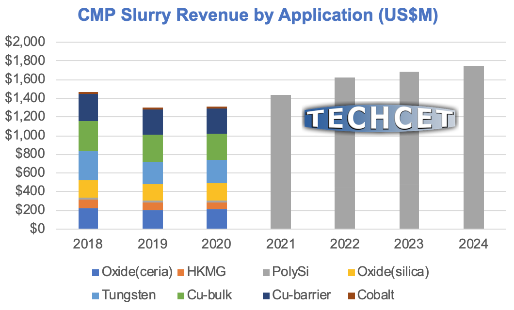
Advanced Packaging and Next Generation Devices Accelerating CMP Consumables Growth
2021 Slurry Market is Forecasted to Reach US$1.80 B up 8% from US$1.66 B in 2020
San Diego, CA, August 3, 2021: TECHCET—the electronic materials advisory firm providing business and technology information— announced CMP (chemical mechanical planarization) consumables for advanced packaging exhibited high growth of approximately 14.1% in 2021 over 2020 and expected to grow at a CAGR of 12.7% over the next 5 years. Applications such as 3DTSV, and FOWLP represent solid opportunities for CMP, adding 1 to 2 CMP steps per wafer.
“In addition to the advanced packaging segment, we are seeing high growth of CMP consumables in next-generation logic and memory devices. The number of CMP process steps continues to increase, driving healthy growth over the next 5 years,” said TECHCET’s President, Lita Shon-Roy. 3D 7nm logic devices require as many as 45 CMP steps, while 3D NAND 128L devices have ~ 34 CMP process steps. These continue to increase as more layers and CMP steps are added into each new generation.

As indicated in TECHCET’s newly released Critical Materials Report™ on CMP Consumables 2021, the total slurry market is forecasted to reach US$1.80 B in 2021 up 8% from US$1.66 B in 2020, with a 5-year CAGR of 6%. Cu bulk, Cu barrier, tungsten, and oxide (both ceria and silica-based) slurries represent the largest segments of the slurry TAM. The resurgence of tungsten slurry growth is being fueled by the rapid increase in layers for 3D NAND. New applications related to HKMG and Co continue to grow as well.
CMP has continued to be one of the critical process steps that make ultra-flat and smooth surfaces enabling advanced electronic device manufacturing with an increasing number of thin layers. The consumables industry fared well during COVID. Despite concerns about an economic slowdown caused by the Covid-19 pandemic, the CMP consumables industry remains strong and is seeing growth as a result of the overall Semiconductor boom. The 2021 pad market is forecasted to reach US$1.11 B up 9% from US$1.02 B in 2020, with a 5-year CAGR of 5.1%.
For more information on the CMP Consumables Critical Materials Report™: https://techcet.com/product/cmp-slurry-and-pads-only/
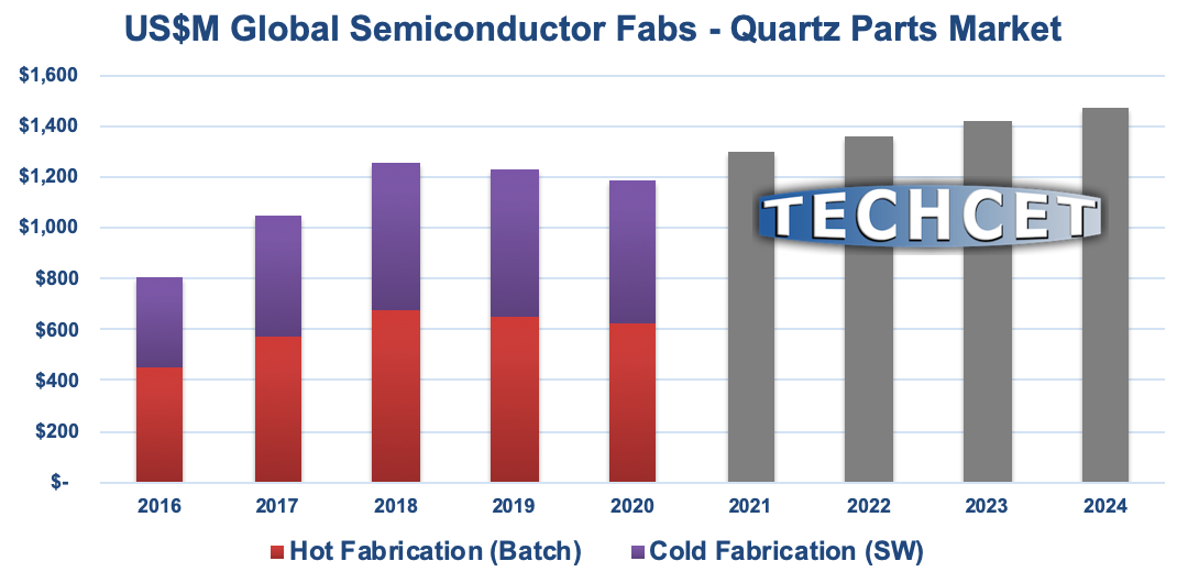
Automotive Market Driving Growth for Legacy Quartz
Quartz Market Is Expected To Reach US$1.66 B in 2021 up ~20%
San Diego, CA, July 13, 2021: TECHCET —the electronic materials advisory firm providing business and technology information— the automotive chip shortage is driving strong growth of < 200 mm quartz demand. Quartz suppliers have been struggling to ramp up production to meet demand. As Highlighted in TECHCET’s Quartz Report. “Even 150mm parts demand is coming back,” stated Lita Shon-Roy, TECHCET’s President & CEO. “The industry is scrambling to provide enough needed components, including silicon carbide, silicon as well as quartz components to support etch and deposition equipment/processes.”
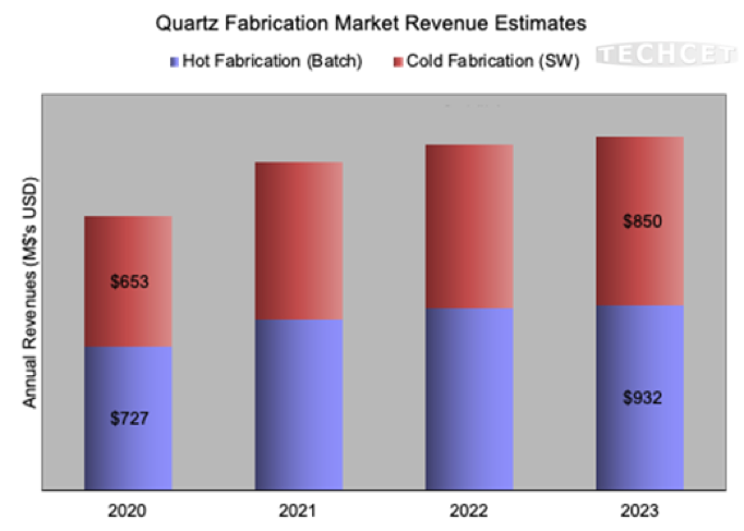
The quartz fabrication market is expected to reach US$1,656M in 2021, growing ~20% from 2020. The 5-year CAGR (2020-2025) for both the base materials and fabricated parts market segments is estimated to be approximately 8%. In 2021, the semiconductor equipment market is expected to exceed 20% further driving demand of quartz parts. The industry will be able to meet the growing demand until 2022, by which time the next wave of quartz supply chain expansion will be needed.
Market shares have only changed slightly. Fabrication market leaders include: Heraeus-ShinEtsu/Conamics, Tosoh, Wonik QnC, Ferrotec, Hayward Quartz, Techno Quartz and Maruwa. With regard to base materials, Wonik’s acquisition of Momentive has improved its position. Major based material shareholders include: Heraeus/Shin-Etsu, Wonik, Feilihua, Tosoh, and QSIL.
Details on the Quartz fabrications market and supply-chain, including base materials and high-purity quartz powder, can be found in TECHCET’s newly released “Critical Materials Report™ on Quartz Parts.”
Critical Materials Reports™ and Market Briefings: https://techcet.com/product/quartz-equipment-components/
Shortage Threat to Semiconductor Materials from US Chip Expansions Plans
Is the US Wet Chemical Supply-Demand out of Balance?
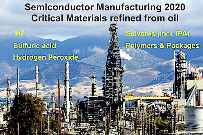
San Diego, CA, July 8, 2021: TECHCET—the electronic materials advisory firm providing business and technology information— warns that semiconductor materials are at risk of shortage in the US. In response to President Biden Executive Order on America’s Supply-Chains, TECHCET submitted a report highlighting US semiconductor material supply-chains at risk. The oncoming expansions planned in the US by Intel, TSMC, Samsung, and others will push up demand and strain the materials supply-chains further. Those materials most vulnerable include wet chemicals, solvents, photoresists, gases, and wafers/substrates. In particular, ultra-high purity wet chemicals are in threat of running short unless additional capacity is put in place.
US Semiconductor device production over the past two decades has declined significantly from 37% of worldwide output to 12%. Now with the potential increase of 30% in US chip production over the next 3-5 years from the top 3 IC manufacturers, materials availability will tighten and may become critical. TECHCET projects that increase in domestic capacity are critical to avoid shortages. Given the time required to bring a new plant online, the time frame for new capacity is now. Note: It typically takes 2-3 years to build a plant to support semiconductor quality chemicals, given all the steps involved in the process. If capacity is not expanded soon, there may be shortages experienced by 2023.

The wet chemicals supply-chain is of highest risk because of several key variables:
- 40% increase in volume demand by 2025
- Lack of additional domestic capacity
- Increasing dependencies on Asian suppliers
- Transportation challenges and rising costs, including ocean freight, and
- Container, storage, and warehousing challenges impacting cost and quality
At present, the US Semiconductor market gets 31% of its Ultra High Purity (UHP) chemicals from Asia. Continued dependency on overseas chemical manufacturing means that as the US chip industry ramps, device manufacturers will be ever more dependent on very long, sometimes fragile supply-chains.
US supply and capacity for chemicals such as semiconductor grade purity sulfuric acid (H2SO4), hydrochloric acid (HCl), isopropyl alcohol (IPA), hydrogen peroxide (H2O2), hydrofluoric acid (HF), phosphoric acid (H3PO4), ammonium hydroxide (NH4OH), and nitric acid (HNO2), has been running at parity with demand. Few to no domestic sources of these chemicals have announced plans to invest in additional capacity, given low margins relative to the high cost of new facilities. As pointed out by Lita Shon-Roy, TECHCET’s President & CEO, “These materials continue to have US supply-chain shortages every other year, if not every year, wreaking havoc on US and European chip fabricators. Without growth in the US wet chemical supply-chain, the US semiconductor industry will continue to have shortages and availability issues, limiting chip expansion plans.”
US Expansion Plans Reliant On Imports
TECHCET estimates 14% of all US Semiconductor Wet Chemicals are supported by Imports. However, when considering only UHP products for leading-edge chip production, this number jumps to 31%, as stated in TECHCET’s latest study, Impact of US Chip Expansion on Wet chemical Supply. The need to import products such as IPA and H2SO4 is a clear indication of the shortcomings of the US UHP supply-chain. As shown in the figure, approximately 100% of all UHP IPA demand is supported by imports. The majority of chemical products coming from overseas are UHP grade because the US has very little ultra-high purity manufacturing capability for many of the semiconductor wet chemicals.
Although many chemical manufactures hesitate to add or build new capacity in the US, it is evident from TECHCET’s research that given the volumes anticipated, the costs to expand chemical production facilities should be justifiable. The key issue will be whether the IDMs will make enough of a commitment for the chemical supplier to invest in new capacity before supply shortages become critical. Failure to further expand US domestic critical materials manufacturing will likely hinder US chip expansion plans.
For more information about US materials supply-chain risks, contact TECHCET on how to get a copy of: “Impact of Chip Expansion on US Chemical Supply-Chain” https://techcet.com/product/impact-of-chip-expansion-on-us-chemical-supply-chain/
Are There New Opportunities for Tier 1 and Tier 2 CVD/ ALD Precursor Suppliers?
Precursors global market is expected to be US$1.7B by 2025.
San Diego, CA, June 29, 2021: TECHCET—the electronic materials advisory firm providing business and technology information— announced announced that there are several new opportunities in the wake of the Pandemic and unresolved Global trade issues for both Tier 1 and Tier 2 suppliers.
- Global fab expansions drive demand and R&D investments
- Continued M&A by Tier 1 suppliers reduce the number of local Tier 2 suppliers, opening up opportunities for start-up activities and smaller entities.
- Continued device design shrink requires the introduction of higher conductivity metals compatible with contact, local interconnects, and BEOL – Mo, Ru, and Ir.
- Continued focus on new lithography and patterning technologies opens new application for dry resist and new hard mask materials to support EUV.
- Multi Patterning development also continues, in search of lower temperature deposition materials.

CVD/ALD Metal and High-k Precursors totaled US$624 million in 2020 and is expected to grow 12% in 2021 to US$710M, as highlighted in TECHCET’s Critical Materials Reports™ on ALD/ High K Metal Precursors and Dielectric Precursors. The 5-year CAGR (2020-2025) is estimated to be 8.0%. The key drivers for growth for various segments are:
- High-κ precursors – DRAM (90 nm and below)
- HKMG: Logic (45 nm and below),
- Tungsten (W): 3DNAND
The highest revenue growth will occur in metal precursors that include:
- Cobalt in Logic
- Ruthenium in Logic, if implemented in high volume manufacturing
- Hafnium in Memory (DRAM and emerging NVM)
- Lanthanum for HKMG
Advanced Dielectric Precursors totaled US$549 M for 2020 and is expected to grow 14% in 2021 to US$624M. The 5-year CAGR (2020-2025) is estimated to be 6.1%. The highest revenue growth will occur in dielectric precursors that support multi-patterning and newer applications areas including EUV, as follows:
- DIPAS/BDEAS precursors: Logic and DRAM patterning (SADP, SAQP)
- TSA: for 3DNAND and potentially also for EUV dry resist (SiN PEALD) in competition with a new precursor based on diiodosilane
This year, STREM was acquired by Ascensus Specialties. M&A activity of large companies is often focused on growing current product lines much to the neglect of R&D activities. Many large companies focus on acquisition to bring in new technology. TECHCET has seen an increase in consulting requests on the ALD/CVD market from potential new entrants.
Critical Materials Reports™ and Market Briefings: https://techcet.com/product/high-kald-precursors/
Critical Materials Reports™ and Market Briefings: https://techcet.com/product/dielectric-precursors/
Wafer Supply Constrained Through 2024 Likely
Will there be new greenfield projects to help with tightened capacity?
San Diego, CA, June 22, 2021: TECHCET—the electronic materials advisory firm providing business and technology information— announced that the wafer supply will remain constrained into and possibly through 2024. With 300 mm wafer capacity tightening, it will likely remain tight in subsequent years unless greenfield capacity is brought online. Based on current forecasts, 300 mm prime wafer demand will be at >99% of utilization production capacity in 2022. Epitaxial capacity utilization is also likely in the 99% range currently. Global 300 mm wafer production capacity will need to expand by 6% or more over the next two years to avoid a shortage in meeting the current 300 mm wafer shipment forecast. However, no new plants have been announced, which means that large capacity additions (if investments/building plans started today) will not happen until 2024 at the earliest. With so much need for growth, new investment for 300 mm greenfield will cost at least US$2 billion and take 2+years to complete before production will be able to start. In addition, suppliers have announced new greenfield investments will require LTAs based on higher pricing.

Larger fab customers likely will not feel the full impact of supply constraints and higher prices. However, the impact is likely to be more significantly experienced by “second-tier” customers.
For 300 mm wafers, “robust” reclaim and reuse efforts in place to reduce demand for test and monitor wafers. This reduces the need for wafer suppliers to support these wafer products. There is upwards pricing pressure reported in the market, including for 150 mm and 200 mm wafers.
- Where will new greenfield investment by the top-tier suppliers occur?
- New greenfield projects will likely be in Japan and in Southeast Asia, where electricity costs are lower.
- Perhaps with funding through the U.S. Chip Acts, there will be an opportunity for 300 mm wafer manufacturing in the U.S. to support the planned fab investments announced by Intel, Samsung, and TSMC.
- New greenfield projects will likely be in Japan and in Southeast Asia, where electricity costs are lower.
Critical Materials Reports™ and Market Briefings: https://techcet.com/product/silicon-wafers/
2021 Resist revenues to grow 6% to $2.0B and to $2.4B by 2025
EUV and KrF materials will continue growing through 2025 given continued ramping of leading-edge devices
San Diego, CA, June 8, 2021: TECHCET—the electronic materials advisory firm providing business and technology information— announced 2021 resist revenues are forecasted to grow 6%+ to $1.98B USD and to continue expanding to $2.37B in 2025. Market dynamics will continue to drive photoresist material revenues upward due to high chip demand and low chip supply.
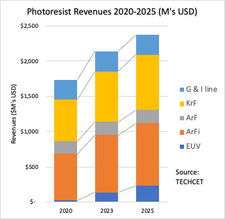
- EUV
- to increase ~90% to $51M for 2021
- volumes nearly doubled from 18 Kliters in 2020 to 35 Kliters in 2021.
- Revenues 53% CAGR 2020-2025
- Driven by leading edge logic and DRAM <5nm
- 2021 KrF driven by 3D NAND
- revenues to and volumes to increase to ~12% in 2021
- I and g-line: up 2-3% for 2021
With the expansion in 3DNAND and logic production over the next 3-5 years, so will the use of photoresist thinner and EBRs which heavily rely on propylene glycol methyl ether acetate (PGMEA), the predominant casting solvent.
Technology trends to watch:
- EUV lithography is in high volume production (HVM) at TSMC and Samsung logic fabs. Intel is expected to start production with EUV in 2021, which will drive EUV ancillaries and photoresist volumes.
- Samsung Electronics is planning mass production of D1z process DRAM using EUV lithography.
- 3D NAND device sales growth and node changes, creating more exposure levels, will drive increases in KrF resist usage, specifically for the thicker formulations, in the ~20% range 2022-2025.
- Directed Self Assembly (DSA) has been demonstrating promising results ; lower defectivity and applicability to lithography pattern repair. This technology is making the sort of progress that portends a future applicability to high volume chip manufacturing.
- Nanoimprint (Canon) has shown improved defectivity and overlay capability and is being yield tested for use in production of 3D NAND memory.
Critical Materials Reports™ and Market Briefings: https://techcet.com/product/photoresists-and-photoresist-ancillaries/
ALD/CVD Metal Precursors US$640M Market Booming to US$910M in 2024
Both advanced logic and memory growing demand
San Diego, CA, April 5, 2021: TECHCET—the electronic materials advisory firm providing business and technology information—announces that the global market for atomic-layer deposition (ALD) and chemical-vapor deposition (CVD) metal precursors for semiconductor manufacturing in 2020 was worth ~US$640M. Driven by advanced logic and 3D-NAND memory chip fabrication needs, demand for ALD and CVD metal precursors is forecast to see a 2020-2024 compound annual growth rate (CAGR) of ~10% as shown in the Figure (below) from the most recent quarterly update to TECHCET’s Critical Materials Report (CMR) on CVD, ALD, and SOD Precursors.
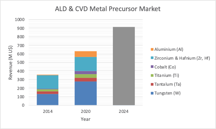
In the short term forecast, TECHCET sees the global semiconductor market as very healthy with 15-20% Year-over-Year (YoY) growth in 2021 revenues, and overall critical materials market growth >7% YoY. The greatest material demand increases are seen in ALD/CVD metal precursors, and in specialty wet cleans that often are integrated with metal deposition and etching.
All ALD/CVD metal precursors are in healthy demand, since ALD is critical for fabs running 22-45nm nodes as well as for fabs at the leading edge. In particular, cobalt (Co) and hafnium (Hf) precursors saw 18-20% year-over-year (Y0Y) growth in 2020, and are forecasted to see strong demand through 2024. Ruthenium (Ru) metal is slowly replacing some of the Co and tungsten (W) interconnects on the most advanced logic chips, with anticipated precursor revenue growth to US$10M in 2025 for this highly strategic material.
ALD materials and Original Equipment Manufacturer (OEM) tools are needed for multi-patterning lithography used with Deep-UV (DUV) Immersion and with Extreme-UV (EUV) in leading logic and memory fabs. Multi-patterning typically uses low-temperature Plasma-Enhanced ALD (PEALD), either in clusters of 8-16 single-wafer chambers, or in “Spatial” high-throughput tools. TECHCET anticipates that fab investments in Asia will allow South Korean and Chinese OEMs to win near-term ALD orders, and they may soon compete with US, EU, and Japanese OEMs in the global tool market. For more information on the impact of global fab capacity expansions on the regional demands for critical materials, please contact TECHCET at [email protected].
Critical Materials Reports™ and Market Briefings: Purchase Reports
2021 Critical Materials Council (CMC) Conference, happening April 14-15 in virtual space, includes presentations on ALD/CVD : 2021 CMC Conference
Photoresists Revenues to be Up 11% to US$1.9B
San Diego, CA, February 23, 2021: TECHCET—the advisory services firm providing electronic materials information—announces that the global market for photoresists needed in commercial semiconductor manufacturing is expected to be worth over US$1.9 billion in 2021. After pandemic-related slowdowns last year, leading semiconductor fabrication lines are now running at full capacities with steady growth expected for the next few years. The fab photoresist market is forecasted to grow 11% year-over-year (Yo) in 2021, as detailed in the latest Critical Materials Report™ (CMR) quarterly update on Photoresists & Ancillaries (see Figure).
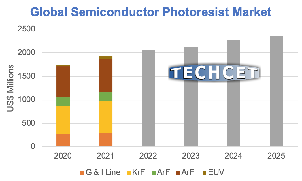
With EUV use in commercial IC fabs now expanding from just advanced logic to include dynamic random access memory (DRAM) chips, the forecast for materials demand growth remains aggressive. ASML claimed capacity in 2020 to build 35 NXE:3400 series steppers, and with anticipated assembly efficiency improvements should be able to ship 50 EUV tools in 2021. Estimated EUV resist sales last year doubled to over US$20 million, and extreme growth in demand calls for these strategic materials to be worth over US$200 million in 2025.
Partly due to trade-wars, China’s 14th five-year-plan published at the end of October 2020 includes a priority to strengthen the country’s independent ability to control industrial supply-chains. Many Chinese states are providing significant funding to develop local production of high-tech materials, and Chinese materials suppliers are sampling photoresists, extensions, and ancillary materials.
This report covers the following suppliers: Avantor, BASF, Brewer Science, Dongjin Semichem, Dongwu Fine-Chem, DuPont (formerly Dow), Eastman Chemical, FujiFilm, JSR, Kempur, KMG (Cabot Microelectronics), Merck/EMD, Moses Lake Industries, Nissan Chemical, PhiChem, SACHEM, Shin-Etsu, Soulbrain, Sumitomo, Suntific, Tama Chemical, Tokyo Ohka Kogyo, and Versum.
Purchase Reports Here: TECHCET Photoresist and Ancillaries Reports
CMP Consumables US$2.9B in 2021 for IC Fabs
High growth in demand for logic and memory 3D metal
San Diego, CA, February 17, 2021: TECHCET—the electronic materials advisory firm providing business and technology information—announces that the global market for chemical-mechanical planarization (CMP) consumable materials in semiconductor manufacturing is expected to grow over 13% year-over-year (YoY) to US$2.93 billion in 2021. CMP consumables including slurries, pads, and conditioning disks are all in high demand due to the need for more planarization steps with 3D devices, and supplies are stable despite COVID-19 pandemic disruptions. CMP materials revenues are forecasted to have a compound annual growth rate (CAGR) of 7.3% as shown in the table from TECHCET’s quarterly update on CMP Consumables: Slurry, Pads, and Conditioning Disks Markets for Semiconductor Applications report (below).
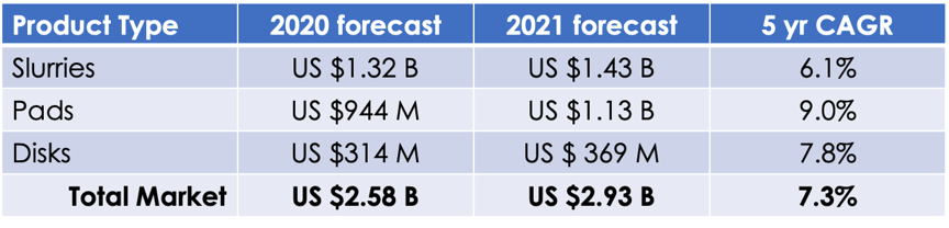
While there has been recent growth in demand for CMP on 200mm silicon wafers, most of the escalating demand today and for the near future is in CMP of metals on 300mm wafers. For logic chips, the largest demand segments are for copper (Cu)-bulk as well as Cu-barrier since the number of Cu interconnect levels on an advanced logic chip continues to increase, despite cobalt (Co) and ruthenium (Ru) gradually being used. For memory chips, increases in the number of layers in 3D-NAND chips drives continued rapid growth in demand for tungsten (W) slurry.
3D-NAND chips rely on W metal for reliable wordline contacts to staggered “staircase” pads within the many layers. Depending upon the manufacturing strategy 64-128 layers is the most that can be economically processed, such that commercial 3D-NAND fabs have to start stacking “tiers” of layer sets. Each additional tier requires additional CMP, so the demand for W CMP is increasing more than the silicon wafer starts.
The CMP consumables market is seeing increased focus on localization of the supply-chain, as global buyers re-examine their value-chains. South Korean giant SKC built a CMP pad manufacturing plant in Cheonan last year, and the plant is scheduled to be put into operation in the second quarter of this year.
Critical Materials Reports™ and Market Briefings: TECHCET Reports
CMC Events: CMC Conference 2021
Semiconductor Materials $50B Market on a Strong Run in 2021
Pandemic pushing people to Work From Home and School From Home
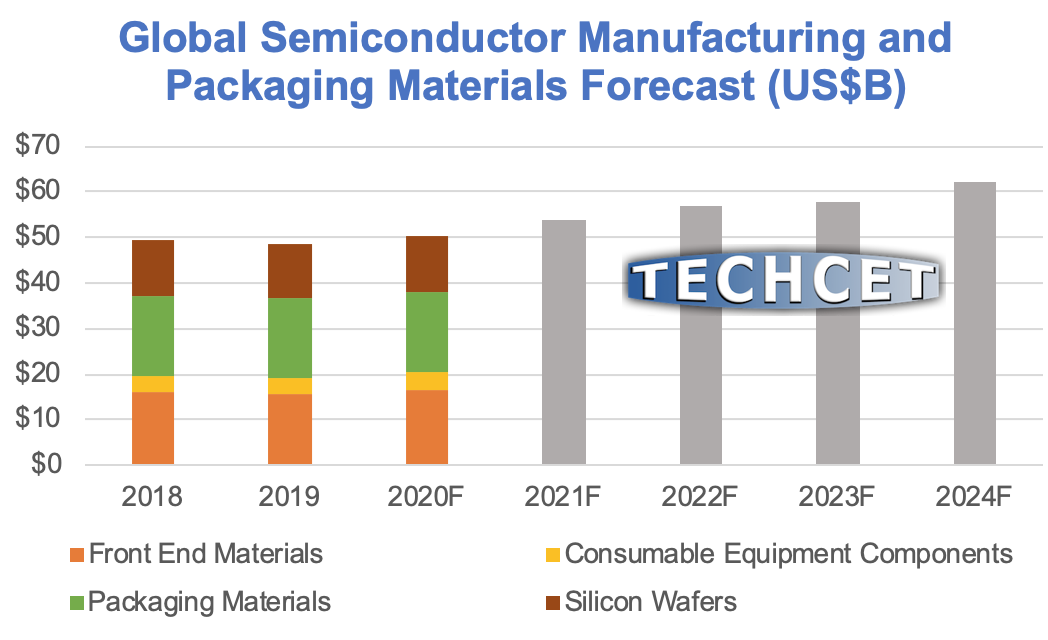
San Diego, CA, January 12, 2021: TECHCET announced that global revenues for semiconductor manufacturing and packaging materials grew approximately 4% year-over-year (YoY) in 2020 to ~US$50B, and are expected to grow ~7% in 2021 to nearly US$54B. The COVID-19 pandemic has created strong demand for both logic and memory ICs to support Work From Home (WFH) and School From Home (SFH), and such demand is expected to increase despite expanding availability of virus vaccines. Also, demand for automotive ICs has recovered and will be an important driver in 2021 growth. The compound annual growth rate (CAGR) through 2024 is forecast at 5.3% as per the latest TECHCET Critical Materials Reports (CMR) and shown in the attached figure.
“Localism is an ongoing global trend, with China, the European Union, South Korea, Taiwan, and the United States all investing in electronic materials capacities due to embargoes and tariffs disrupting supply-chains,” said Lita Shon-Roy, TECHCET President and CEO. “Even without political disruptions, critical materials for the fabrication of advanced logic and memory chips such as cobalt and lanthanum have been in short supply due to competing industrial demands, and we expected tightening supply of silicon wafers in 2021.”
Such ramifications are tracked by TECHCET’s analysts, with Analysts’ Alerts emailed to CMR purchasers to help them anticipate and mitigate potential supply-chain disruptions. Excerpts have been publicly disclosed on the following critical materials (click here to read the full stories):
• IPA in “CMC Considers Bio-Solvents to Reduce Fab Risks”,
• HF in “Semi Wet Chemicals US$2B Market Threatened by Localization”, and
• Lanthanum in “Rare Earth Elements (REE) Supply Uncertain for IC Fabs”.
Any switch in material source triggers the need to re-qualify with cycles of test wafers and rigorous metrology, and similar data are needed during chip fabrication to ensure that material quality is under control. The public 2021 CMC Conference—happening April 14-15, 2020 in virtual space—is now soliciting presentations on themes surrounding semiconductor fab materials quality and metrology issues.
Critical Materials Reports™ and Market Briefings: TECHCET Reports
CMC Events: CMC Conference 2021
CMC Considers Bio-Solvents to Reduce Fab Risks
Semiconductor Grade IPA Supply Impacted by COVID-19
San Diego, CA – December 21, 2020: The Critical Materials Council (CMC) of semiconductor fabricators & suppliers joint-meeting in December focused on disruptions in the global supply-chain for high-purity acids and solvents due to the boom-and-bust business of oil refining. Due to COVID-19 pandemic travel restrictions reducing passenger travel, there has been a well-documented reduction in demand for oil and gasoline that has led to the idling of some petroleum refineries. Much of the world’s industrial chemical supply starts with petroleum feedstocks, so when refineries stop running they stop supplying the world with raw material.
As shown in the Figure, wet chemicals including sulfuric acid, hydrogen peroxide, and iso-propyl alcohol (IPA) are typically engineered these days using feedstock from oil refining derivatives. During the December CMC Joint Session of chip fabricators and suppliers, a representative from Cargill Corporation (annual revenues ~US$114B) presented information on sustainable bio-based feedstocks that can replace petrochemicals in the global supply chain.
TECHCET material demand models estimate that 2020 worldwide semiconductor device fabrication will use and dispose of the following:
• 291 million kg of sulfuric acid or 760,000 55-gallon drums,
• 202 million kg of hydrogen peroxide or 857,000 55-gallon drums, and
• 20 million kg of IPA or 122,000 55-gallon drums.
Earlier this year, TECHCET raised “cautionary flags” at CMC meetings to watch for 2H20 shortages of IPA and sulfuric acid, as also detailed in quarterly updates to TECHCET’s Wet Chemicals & Specialty Cleans analysis. Governments around the world have mandated that some of the industrial IPA supply-chain be re-directed to healthcare and consumer distribution to combat the COVID virus, increasing overall demand. French IPA producer Seqens had to declare force majeure on its IPA plant in Peage, Roussillon from March to July of this year, and with a nameplate capacity of 70k tons/year that plant represents >12% of total European capacity. Despite recent news of vaccines, the pandemic continues to disrupt the chemistry value-chain.
During the December 8, 2020, CMC meeting, Fab Members from around the world reported tightening supply of high-purity solvents in general. Within the solvent category, there is now serious concern that a shortage in high-purity IPA is looming just over the business horizon. To join the CMC for 2021 meetings in virtual-space to anticipate and mitigate such supply-chain disruptions, or for custom consulting please contact us – Email, +1-480-332-8336.
For more information on solvents, wet chemicals, and other critical materials used for semiconductor production: TECHCET Reports
Semi Wet Chemicals US$2B Market Threatened by Localization
Specialty Cleaning and Etching Changes Could Cause Yield Losses
San Diego, CA, December 1, 2020: TECHCET—the electronic materials advisory firm providing business and technology information—announces the global market for wet chemicals needed for global semiconductor fabrication in 2021 is forecast to reach US$2 billion. However, recent trade wars threaten the stability of global supply-chains for critical materials, with China, the European Union, Japan, and the U.S. all announcing plans to create parallel local sources for electronic materials, and South Korea and Taiwan increasing investments in chemical production. There are many specialty blends needed as well as ultra-pure neat chemicals, and all are growing in demand as seen in the Figure (below) from the latest Critical Materials Report™ (CMR) quarterly update on Wet Chemicals & Specialty Cleans.
The most advanced IC fabs for logic and memory chips require purity levels in materials so extreme that trace contaminants below parts-per-billion can cause millions in dollars of commercial yield losses. When raw materials sources or refining processes change there are corresponding changes in the trace contaminants and the chemical fingerprint so semiconductor fabs require that suppliers use advanced metrology and sophisticated analytic methods to re-qualify any changes.
“Advanced commercial ICs can only be profitably fabricated when the critical materials supply-chain is locked in from the very beginning at the mine or other industrial feedstock,” explained Terry Francis, TECHCET Director of Technology and Senior Analyst and author of the report. “For anhydrous-HF supply, we’re seeing a shift in the fluorine source from fluorspar mining to alternates including FluoroSilicic Acid (FSA), depleted uranium hexafluoride, and aluminum fluoride. All of these alternates will have different trace contaminants which will have to be re-qualified by fabs.”
SK Materials began mass producing 15 tons-per-year of ultra-high-purity (UHP) hydrogen fluoride (HF) gas at its in Yeongju, South Korea to support fabs and help reach the government’s goal of 70% local electronic materials supply by 2023. South Korea’s imports from Japan have been replaced to a great extent by an increase in imports from China and Taiwan.
In China, Wengfu has four plants producing Anhydrous-HF (AHF) from FSA, with a fifth plant due to come onstream by early 2021. The company claims that the total capacity of all five plants will be ~105,000 tons/year AHF produced using this route.
This wet chemical market report covers these suppliers: Arkema, Avantor, BASF, Cabot Microelectronics/KMG, CF Industries, Dow/DuPont, Eastman, Evonik, GrandiT, Hansoi Chemical, Hubei Sinophorous, Jianghua Microelectronics Materials, Kanto Chemical, Merck/EMD, Mitsubishi Gas Chemical, PeroxyChem, Rudong Zhenfeng Yiyang, Runma Chemicals, SACHEM, SK Materials, Solvey, Suzhou Crystal Clear, Xingfa, Wengfu.
Critical Materials Reports™ and Market Briefings: Specialty Cleaning Report
Wet Copper Deposition Materials for ICs and Packages
Steady growth in demand forecasted through 2024
San Diego, CA, November 16, 2020: TECHCET announces that the global market for wet metal deposition materials including electro-chemical deposition (ECD) and plating (ECP) chemistry blends in 2020 is forecast to be US$63 million. From semiconductor fabrication at wafer-scale in the Front-End Of Line (FEOL) to wafer-level and die-level advanced packaging, specialized copper (Cu) chemistry blends are seeing compound annual growth rates (CAGR) in demand of 11-13% over the period 2019-2024. While on leading-edge logic chips, cobalt (Co) plating is used to make the smallest connections to transistors, as detailed in the latest Critical Materials Report™ (CMR) quarterly update on Metal Chemicals for FEOL & Advanced Packaging.
While 2/3 of chip packing today still uses relatively simple wire-bonding, TECHCET sees demand for advanced packaging—including flip-chip (FC), fan-in wafer-level packaging (FIWLP), fan-out wafer-level packaging (FOWLP), and through-silicon vias (TSV)—to grow at a strong 8.9% compound annual growth rate (CAGR) over the period 2019-2024 (Figure). These advanced packaging interconnects will continue to use plated solder formulations of tin (Sn) and tin-silver (SnAg), while demand for Cu plating chemistry for interconnect “bumps” and re-distribution lines (RDL) is expected at 11% CAGR over the same period.
“While advanced packaging interconnects are adding more value to final system function, improved metal lines are still needed on most advanced IC chips in heterogeneous integration,” explained Terry Francis, TECHCET Director of Technology and Senior Analyst and author of the report. “On-chip copper metal constrains the speed of the densest ICs today, which has led to use of cobalt in the lower metal layers in 10nm-node and smaller logic devices.”
This report covers the following suppliers: Atotech, BASF, Dow/DuPont, Ishihara, MacDermid/Enthone, Materion, Moses Lake, Soulbrain, Shinhao, Uyemura.
Critical Materials Reports™ and Market Briefings: Metal Chemicals Report
Refreshing Material Advances for Logic, Memory, and Packaging
5th CMC Conference “After-Hours” Available up to December 11
San Diego, CA, November 5, 2020: How to keep semiconductor fabs supplied with critical materials despite a pandemic and trade wars was discussed by >250 industry experts gathered in virtual space October 21-22 during the 5th annual Critical Materials Council (CMC) Conference. CMC Fab Members and Associate Supplier Members were joined by leading industry analysts, educators, and investors in discussing business and technology trends in the value-chain for advanced packaging, logic, and memory. The “after-hours” virtual conversations will continue through December 11th using the conference app and website, and new people can join in through November 16th.
“There were a lot good topics especially on materials challenges for leading edge technology and heterogeneous integration, global issues on material supplies, and emerging materials development,” commented Dr. Lihong Cao, Director of Engineering and Technical Marketing at ASE, and Session 4 presenter.
This was the first year that a new conference session was dedicated to Advanced Packaging of Heterogeneous Integration using chips from different fabs. Dr. Lauren Link of Intel discussed the need to find ways to integrate more front-end fabrication materials into packaging. The challenge is how to do so in a cost-effective manner, without over-specifying materials and process requirements as shown in the screen-capture (Figure).

While materials revolutions are happening in advanced packaging, materials evolutions are also essential to improve reliability and quality. Dr. Alejo Lifschitz of DuPont showed how the clever addition of a new “Grain Refiner” additive to the company’s chemistry blend allows for electro-chemical deposition (ECD) of copper (Cu) lines that have reliability engineered into the micro-structure. As deposited, the new Cu grains for the package Re-Distribution Layer (RDL) are <0.2 micron in size with >93% in maximum density highly-twinned <111> crystallographic orientation. This makes reflowed Cu RDL lines that are inherently more resistant to corrosion and cracking when subjected to chemical and mechanical stresses in the real world.
Advanced Logic: finFETs and NanoSheets
Fin-based Field Effect Transistors (finFET) in the most minimally-scaled logic chips will soon be replaced with Horizontal Nano-Sheets (HNS) to improve device performance. HNS are Gate All-Around (GAA) CMOS FETs that reduce power-consumption while allowing for simple patterning of different gate-widths so that designers can optimize power:performance trade-offs within the IC layout. However, both evolutionary and revolutionary new manufacturing processes will be needed for commercial fabrication of HNS logic ICs.
The best example of a revolutionary new process that is needed to make HNS ICs is that of the epitaxial (Epi) growth of the layers to make the transistor channels. Pamela Fischer of ASM in presenting on, “Materials Evolution and Challenges in ALD/Epi FEOL,” explained that when growing alternating Epi layers the interface transition thickness directly determines final device performance. The company’s latest Epi tool allows for alternating ~10nm thick layers of silicon (Si) and silicon-germanium (SiGe) to be grown with extremely sharp transitions of just ~0.5nm. This means that the transition happens in ~2 atomic layers of silicon!
Advanced Memory Materials
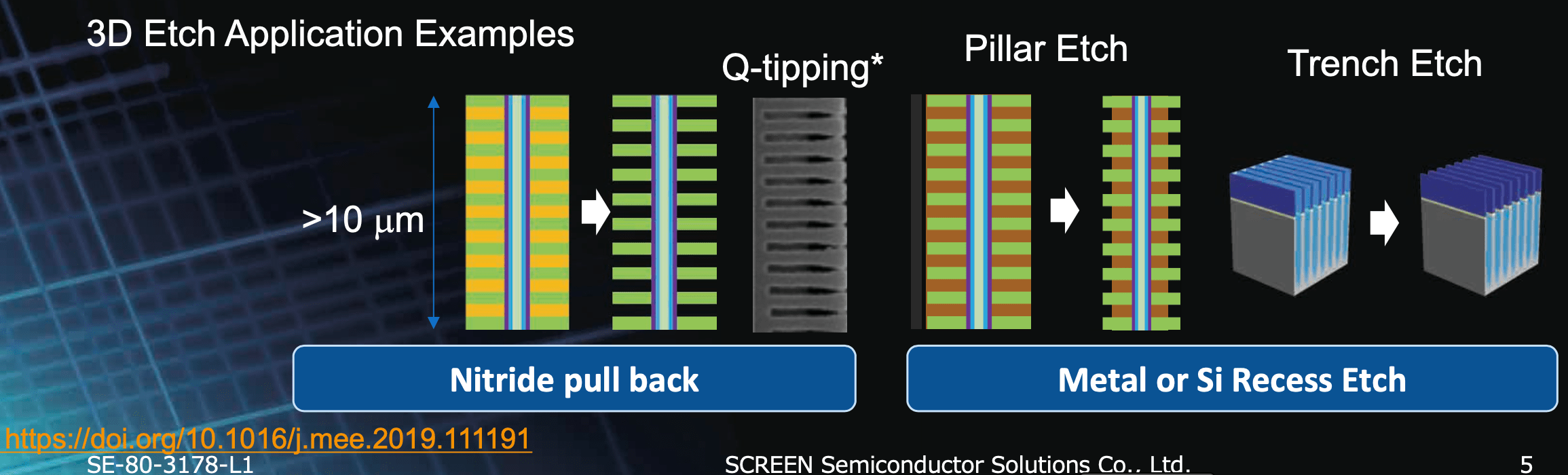
3D device fabrication issues in logic fabs pale in comparison to the ongoing challenges with finding integrated process flows for 3D-NAND memory chips, which currently stack ~100-device-layers and will soon aim for ~200-device-layers on each silicon wafer. Dr. Ian J. Brown, VP Engineering for SCREEN Semiconductor Solutions, showed how “Wet Etching in the 3D Era” has evolved to enable 3D device structures for both logic and memory (Figure). Tools are becoming more sophisticated to allow for chemical blending on-site in the fab, which allows for cost-effective use of more complex chemistry sets. “Digital Wet Etch” (DWE) is a 2-step process similar to Atomic-Layer Etch (ALE), where a first chemistry oxidizes the surface of a metal such as copper (Cu) or cobalt (Co) following which a second chemistry selectively removes just the metal-oxide layer.
Shaun Miller, Director of Global Front End Materials Procurement for Micron Technology, showed why independent regional supply-chains can create, “Material Challenges in Leading-Edge Memory Manufacturing.” For example, differences in supplier infrastructures between the U.S. and Taiwan have led to different levels of metallic and particle impurities in wet chemicals such as sulfuric-acid and hydrogen peroxide, with Taiwan leading in purity at present. Micron is using analytics and “big data” to collaborate on a deeper level with suppliers.
In follow-on conversation, Terry Francis, TECHCET Sr. Analyst who also presented at the conference, explained how hydro-fluoric acid (HF) supply in North America is likely to change in the near term. The raw material supply is changing from mined fluorspar mineral to chemically-engineered fluorosilicate-acid (FSA), since the latter is in surplus as a byproduct of phosphate-based fertilizer production. While electronics manufacturing consumes at most 1% of industrial demand, there is insufficient volume to sustain a supply-chain independent of that for general industry. Such a change in upstream material source would inherently change the trace contaminants in the final downstream HF, which could trigger random yield losses in advanced IC fabs unless materials are carefully re-qualified.
Post-event registration is open until November 16th, so click through to access recordings of presentations and discussions, connect with attendees, and engage in follow-up Q&A!
Critical Materials – PVD Targets US$1B and Growing Strong
Increasing demand forecasted through 2024
San Diego, CA, October 21, 2020: TECHCET—the electronic materials advisory firm providing business and technology information—announces that the global market for Physical Vapor Deposition (PVD) including Sputtering consumable materials in semiconductor manufacturing is expected to total over US$1 billion this year. Demand was strong in the first half of 2020 as fabs built up safety stock in response to COVID-19, and sales momentum continued into the third quarter. 2020 revenues are forecasted to be up 2.1% with even stronger growth in 2021 of 5.9% year-over-year, as detailed in the latest Critical Materials Report™ (CMR) quarterly update on Sputter Targets (see Figure).
“The top five suppliers of non-precious-metal targets control approximately ninety percent of the global market,” explained Dr. Dan P. Tracy, TECHCET Sr. Director of Market Research and author of the report. “This mature materials value-chain supports the world’s needs for on-chip metal interconnects, and TECHCET expects that some consolidation in the market is likely over the next several years through mergers and acquisitions.”
TECHCET sees a long-term trend towards recycling of most metal targets to become an increasingly important part of life cycle management. While precious metals such as gold (Au) and Rare Earth Elements (REE) have always been recycled as much as possible, there are both short-term economic incentives as well as long-term sustainability motivations to recycle copper (Cu), tantalum (Ta), and titanium (Ti).
This report covers the following suppliers: Furuya Metals, GO Element, Grikin, Honeywell, JX Nippon, KFMI, Materion, Pioneer Materials, Praxair/Linde, Sumitomo, Tanaka, Top Metal Materials, Tosoh SMD, Solar Applied Materials Technology, Umicore, VEM, and Vital Materials.
Critical Materials Reports and Market Briefings: TECHCET Shop
5th Annual CMC Conference this week: CMC Events
Semiconductor Materials Market to Hit $50B in 2020 Up 3%
Winds Reverse on the Global Supply-Chain Seas
San Diego, CA, September 21, 2020: TECHCET announces that 2020 global materials revenues in semiconductor fabrication are now forecasted upward year-over-year (YoY) despite potential disruptions to manufacturing:
•  Overall revenues +2.8% to hit over $50B, versus outlook in April for -3%,
•  Front End Materials +5% to hit $16.4B, and
•  Equipment Components +10% to hit $3.8B.
While the impact of COVID-19 on the global economy is serious, IC fabrication is steady for devices to Work From Home (WFH) and School From Home (SFH). As predicted, leading-edge ICs to build out data centers are in strong demand this year, as part of forecasted 5.4% Compound Annual Growth Rate (CAGR) for fab materials through the year 2024 (Figure below).
“TECHCET now sees Front-End Materials volumes and revenues for the year 2020 to be buoyed up by cloud computing and devices to support Work From Home and School From Home,” remarked Lita Shon-Roy, TECHCET President and CEO. “In recent online meetings, the members of the Critical Materials Council of Semiconductor Fabricators have said that most fabs are running at normal levels, while leading-edge logic and memory fabs are actually having a great year.”
Advanced logic fabrication now drives a massive 30% YoY increase in demand for cobalt (Co) deposition precursors. Because of the need for speed and reliability in the most advanced finFET logic chips, the smallest on-chip wires are being converted to cobalt from copper (Cu). Interconnect metallization for semiconductors continues to grow in general, so the demand for copper remains strong albeit somewhat reduced. Sourcing cobalt is still problematic due to conflict-mining in the Democratic Republic of the Congo, yet companies such as Umicore and Australian Mines have gone to great lengths to ensure their sources are conflict-free and sustainable.
Chemical-Mechanical Planarization (CMP) Pad Conditioner revenues for 300mm wafers are growing at 4.5% for 2020, due to 3D-NAND device volume growth and overall equipment sales. CMP processing flattens the surface as device layers are stacked up, and the CMP pad lifetime is increased with corresponding manufacturing cost-reduction by use of specialized diamond-abrasive conditioning disks.
Packaging materials revenues for 2020 should be up >1% due to the relative increase in value of advanced packaging, as more and more chips require interconnects faster than wire-bonds. This is a continuance of the multi-year trend of multi-chip packages using flip-chips and interposers and embedded-bridges. Deep details on packaging materials can be found in the “Global Semiconductor Packaging Materials Outlook” report published by SEMI, TECHCET, and TechSearch, available at the SEMI website.
Critical Materials Reports and Market Briefings: TECHCET Shop
To register for 2020 CMC Conference: CMC Events
CMP Consumables US$2.5B in 2020 for IC Fabs
Stable world-wide growth in demand forecasted through 2024
San Diego, CA, August 27, 2020: TECHCET—the electronic materials advisory firm providing business and technology information—announces that the global market for chemical-mechanical planarization (CMP) consumable materials in semiconductor manufacturing is expected to total over US$2.5 billion this year. CMP consumables including slurries, pads, and conditioning disks are all in stable supply globally, despite COVID-19 pandemic disruptions. The total sub-market just for CMP slurries is forecast to be US$1.3 billion this year, with a Compound Annual Growth Rate (CAGR) of 6.2% per year over the period 2020-2024, as shown in the figure from TECHCET’s 2020 CMP Consumables: Slurry, Pads, and Conditioning Disks Markets for Semiconductor Applications report (below).
While the 2020 CMP slurry market will be down ~2.2% from 2019 levels, ongoing demand for both logic and memory IC fabs is expected to drive steady growth through 2024. For logic chips, the largest demand segments are for copper-bulk, copper-barrier, tungsten, and shallow trench isolation (STI), while slurries for HKMG and cobalt are highly value-added despite relatively lower volume demands. For memory chips, increases in the number of layers in 3D-NAND chips drives continued rapid growth in demand for tungsten slurry as well as ceria slurry for high-rate oxide planarization steps.
“Showa Denko’s recent acquisition of Hitachi Chemical was another sign of a maturing semiconductor materials supply-chain,” commented Dr. Diane Scott, TECHCET Analyst and co-author of the report. “This business unit is the world’s leader in supplying ceria slurry, a highly specialized formulation using Rare Earth Oxide nanoparticles to make ultra-smooth surfaces for the world’s most advanced ICs.”
The CMP consumables market is seeing increased focus on localization of the supplychain, with many suppliers looking at finishing product closer to the end-users. Finishing refers to final production steps of the material, which in the case of pads could include application of adhesives, cleaning, quality control (QC) inspections, and specialized clean packaging for shipment. Benefits include reduced shipping cost, faster customization, and localized buffer-inventory to support demand surges.
Critical Materials Reports and Market Briefings: TECHCET Shop
Rare Earth Elements Supply Uncertain for IC Fabs
China’s de facto monopoly control remains for now
San Diego, CA, July 29, 2020: TECHCET—the electronic materials advisory firm providing business and technology information—announces supply-chain challenges ahead for Rare Earth Elements (REE) for semiconductor device manufacturing, due to ongoing global pandemics and trade-wars. The United States is fast-tracking domestic REE refining capability to provide a global alternative to China’s current de facto monopoly, but it could be 2022 or later before new capacity is available. The global supply of Rare Earth Oxides (REO) is expected to see a Compound Annual Growth Rate (CAGR) of 4.0% per year over the period 2018-2025, as shown in the figure from TECHCET’s 2020 Rare Earths Supply-Chain Report (below).
“Although China is the global market leader for Rare Earth metals, they do not control all the mining in the world,” commented Terry Francis, TECHCET Analyst and author of the report. “By specializing in the difficult refining and separation processes, Chinese companies have maintained a near-monopoly on rare earth metals production. They own most off-take from global mines such that they ship over 83% of the world’s pure rare earth metals.”
TECHCET is tracking three new REE refining operations in the U.S.:
• Lynas Corporation of Australia and Blue Line Corporation in Texas were awarded grants in late July 2020 by the U.S. government to develop a processing plant to extract rare earths from material sent from Malaysia.
• MP Materials will go public in 4Q20 on the New York Stock Exchange at a valuation of US$1.47B where it will trade as “MP.” The company plans to invest US$489M in refining capacity in Mountain Top, California. In April 2020, the U.S. Department of Defense awarded MP a grant to pay for the design of a heavy REE separation facility.
• USA Rare Earth and Texas Mineral Resources started a heavy and light REE refining pilot plant in Wheat Ridge Colorado last December. It is working on a fullscale refinery for REE, lithium and other technology metals in Round Top, Texas.
U.S. refineries are not expected to be capable of volume supply until 2022 or later. In the meantime, China’s REE companies will control the market. China’s government recently announced a 6.6% increase in quota limits on exported volumes for 2020 over 2019. This is good news for REE buyers, but for new suppliers in the U.S. and Australia it likely means that market pricing will not follow traditional supply-demand trends. Pricing is likely to be highly variable, with possibilities of spikes in the spot market.
Another important market factor is that the handling of rare earth waste is challenging. Countries that are considering local refining capabilities must mitigate environmental risks. For example, USA Rare Earths recently announced their intention to rely on renewable energy for all of their power requirements as one way to balance environmental impacts. TECHCET anticipates more announcements inside and outside of China will be made over the next year addressing environmental concerns.
Critical Materials Reports and Market Briefings: TECHCET Shop
Quartz Parts Market for Semiconductor Fabs Downward Trend Expected to US$1.2B
Skilled Labor Shortage for Quartz Tube Fabricator Concerns
San Diego, CA, July 4, 2020: TECHCET—the electronic materials advisory firm providing business and technology information—announces that the market for quartz components and parts used in Original Equipment Manufacturers (OEM) tools is now forecasted to decline 3-5% in 2020 to reach US$1,187M. However, this market is still expected to experience a 4% CAGR from 2019 to 2024 as shown in the figure.
Other highlights from the 2020 Critical Materials Report (CMR) on Quartz Components, Fabricated Parts, and Base Components for Semiconductor Applications include:
• With the COVID-19 pandemic in 1H20, a few large fabs started increasing purchase orders by 15-20% MoM to increase safety-stock levels,
• China’s market experienced mild growth in 2019, since new local suppliers are still climbing a learning curve; only a handful of companies are able to pass qualification as suppliers to top-tier IC fabs,
• Quartz suppliers in Taiwan will generate +15% revenue growth from Taiwan chip fabs which have continuously run throughout 1H20, and
• Although reports of orders in 1Q2020 appear positive, TECHCET expects softening to start occurring in 2H2020 which will effect overall 2020 revenues.
“The global slowdown due to the COVID-19 pandemic is a good time for quartz suppliers to catch up on the talent shortage,” remarked Kuang-Han Ke, TECHCET Analyst and author of the report. “While machined parts capacity can be ramped up easily, quartz diffusion tube supply depends on experienced craftsman and talent. Many of the mid-size quartz fabricators have been able to out-grow the market with strategic hiring.”
During 2018, legacy equipment parts including furnace tubes faced longer lead-times for the second-tier fabs. This was the result of limited hot fabrication production spots taken up to fill orders from larger volume first-tier fabs and OEM equipment demand.
TECHCET sees the hot growth areas for ICs in 2020 to be in foundry logic and memory chips for high-performance computing and ultra-mobiles. Demand for semiconductor quartz components is largely supported by spares sold by local suppliers, though new furnace and etch equipment OEM sales are important market segments.
Critical Materials Reports™ and Market Briefings: TECHCET Shop
2020 CMC Conference – State of the Art Virtual Engaging
5th Annual Materials Event Will Happen in “Virtual Space”
San Diego, CA, July 1, 2020: TECHCET and the Critical Materials Council (CMC) announce that the 5th annual CMC Conference will be delivered “live” October 21-22 weaving worldwide-web services into a valuable digital experience, using a state of the art platform for the best in virtual networking.
The 2020 CMC Conference will feature 4 impactful sessions over 2 days with dynamic Q&A, and will also include a suppliers’ poster session, and Materials Action™ roundtables:
I. Global Value-chain Issues, Including Economics and Regulations,
II. Immediate Challenges of Materials & Manufacturing,
III. Emerging Materials in R&D and Pilot Fabrication, and
IV. Heterogeneous / Advanced Packaging Materials (NEW for 2020).
FEATURED KEYNOTE:
Bruce Tufts, VP Of Technology And Director Of Fab Materials Organization, Intel Corp. presenting “Critical Materials Pushing the Limits for Semiconductor Manufacturing”
30 POWERFUL PRESENTATIONS, INCLUDING THE FOLLOWING:
Dan Hutcheson, CEO, VLSI Research
De-Globalization
Scott Jones, Managing Director, KPMG
Is the World is “On sale”? M&A Activity
Ashutosh Misra, Chief Technology Officer, Electronics at Air Liquide
New Gases for Atomic Layer Etching
Kandabara Tapily, PhD, Member of Technical Staff, TEL
Selective Deposition for Advanced Patterning
Register before August 31st at the Early Bird rate, and optionally select “Advisory Alert Access” to tap into insights from CMC Fab Members and CMC Associate Members on ways to mitigate supply-chain disruptions from COVID-19 and trade-wars.
CMC COVID-19 Impact Survey Shows Supply-Chain Strength
Pre-registrants for 2020 CMC Conference access COVID-19 Info
May 29, 2020: The Critical Materials Council (CMC) of semiconductor fabricators & suppliers is continuing to work to mitigate potential supply-chain disruptions by conducting surveys and holding virtual workshops. The May survey on COVID-19 impacts indicates that the global supply-chain for critical materials is strong, with two-thirds of suppliers reporting no disruptions. The CMC has now opened attendance at monthly COVID-19 Briefings and Virtual Workshops to pre-registrants for the 2020 CMC Conference, happening October 22-23 in Hillsboro, Oregon
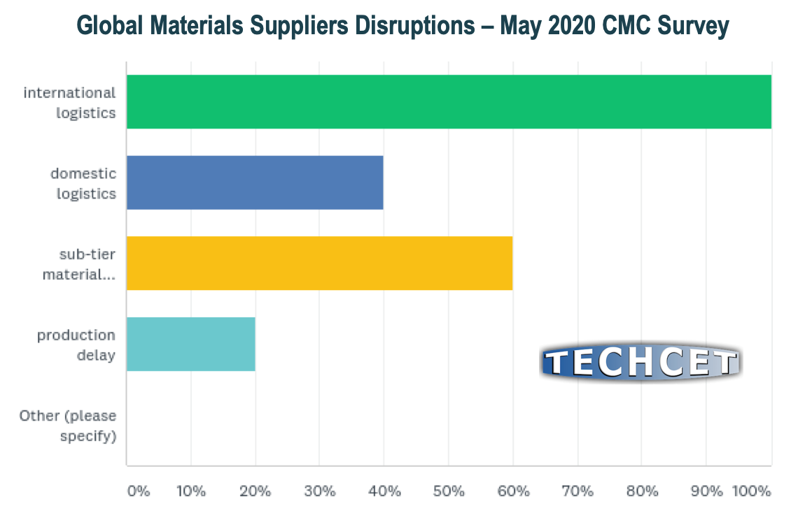
Electronic materials supply companies from around the world responded to this latest CMC survey. About two-thirds of respondents report that they are not currently experiencing any problems with their supply-chains, which reassures fab customers that there should be no disruptions in shipments. However, about one-third (5 respondents) say that there are issues (Figure). Three respondents noted issues with sub-tier suppliers, while two have experienced problems with domestic logistics. TECHCET is tracking renewed interest in establishing parallel local supply-chains for critical materials in all global regions.
The survey shows that 60% of suppliers are increasing their own “safety stock” inventory levels of materials from sub-suppliers. Coincidentally, 60% of suppliers have also restricted all travel by employees, while 20% of suppliers are still traveling to support fab customers. As a strong indicator that the world is now soft-opening from COVID-19 lockdowns, 40% of suppliers now report that customers are visiting their sites, up from 0% in early May. Overall order volumes seem to be the same if not slighter higher than levels one year ago.
BRIEFINGS AND VIRTUAL WORKSHOPS
By pre-registering for the 2020 CMC Conference now, you can attend the next interactive COVID-19 Virtual Workshop on June 24th. These monthly meetings consolidate what is happening now in critical value-chains and provide forecast updates for strategic planning. Pre-registrants will also be able to access news and analysis at the CMC information website.
Daily and weekly analysis at this website on the impact of COVID-19 on semiconductor materials markets and supply-chains includes:
• TECHCET briefings and statistics,
• Global news relating to semiconductor materials,
• CMC Fab Members and Supplier Associate Member survey results, and
• Credible web resources for information on the growing pandemic.
2020 CMC Conference
Featuring a Keynote by Bruce Tufts, VP of Technology and Director of Fab Materials Organization, Intel Corp. on “Critical Materials Pushing the Limits for Semiconductor Manufacturing” the 5th annual CMC Conference will include more than 25 powerful presentations, the popular Materials Action™ roundtables featuring discussions and refreshments, and other networking opportunities.
CMC Workshop Flags Looming Shortages of IPA and Sulfuric
Pre-registrants for 2020 CMC Conference access COVID-19 Info
These extraordinary times of greater risks call for more information, so the Critical Materials Council (CMC) of semiconductor fabricators & suppliers is now meeting briefly several times a month to exchange pre-competitive information to mitigate potential supply-chain disruptions. The last meetings exposed a likely shortage in iso-propyl alcohol (IPA) looming just over the business horizon due to the COVID-19 pandemic. The CMC has now opened attendance at monthly COVID-19 Briefings and Virtual Workshops to pre-registrants for the 2020 CMC Conference, happening October 22-23 in Hillsboro, Oregon
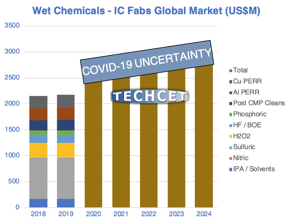
Fabs and suppliers say that the supply-chain for semiconductor-grade IPA has the capacity to meet current global requirements (Figure). However, due to COVID-19, governments around the world have mandated that some of the industrial IPA supply-chain be redirected to healthcare and consumer distribution, increasing overall demand. Spot prices for this critical material have reportedly increased a staggering 30% month-over-month (MoM).
Global sources of IPA depend on propene feedstock from oil refiners, and the current economic slowdown has reduced oil demand to such an extent that refineries are being idled. TECHCET has put up “cautionary flags” to watch for 2H20 shortages of IPA and sulfuric acid, as per the latest quarterly update to TECHCET’s Wet Chemicals & Specialty Cleans analysis.
While regional disruptions to IPA supply are nearly certain in the short-term, global materials companies are responding by trying to increase shipments. For example, industry sources indicate that an Asian supplier of IPA is now trying to move material to the US and Europe. In the last COVID-19 Virtual Workshop of the CMC, attendees discussed the ramifications of a reduced number of ships leaving ports around the world, and why they anticipate that the average time to ship cargo will increase.
BRIEFINGS AND VIRTUAL WORKSHOPS
The next COVID-19 Briefing will be given on May 6th, and the next interactive COVID-19 Virtual Workshop will happen on May 27th. Pre-registrants for the 2020 CMC Conference will be able to join in these monthly meetings to learn what is happening now in critical supply-chains, and will also be able to access updated news and analysis archives at the CMC information website. This website (https://criticalmaterials.org/covid-19/) aggregates daily and weekly analysis on the impact of COVID-19 on the semiconductor materials markets and supply-chains. Four folders of
information are provided which include:
-
- • TECHCET Briefings and Statistics,
-
- • Global News relating to semiconductor materials,
-
- • CMC Fab Members and Supplier Associate Member survey results, and
- • Credible web resources for information on the growing pandemic
2020 CMC Conference
Featuring a Keynote by Bruce Tufts, VP of Technology and Director of Fab Materials Organization, Intel Corp. on “Critical Materials Pushing the Limits for Semiconductor Manufacturing” the 5th annual CMC Conference will include more than 25 powerful presentations, the popular Materials Action Roundtables with discussions and refreshments,
and other networking opportunities.
Four impactful presentation sessions will cover:
I. Global Value-chain Issues, Including Economics and Regulations,
II. Immediate Challenges of Materials & Manufacturing,
III. Emerging Materials in R&D and Pilot Fabrication, and
IV. Heterogeneous-Integration / Advanced Packaging Materials.
The fourth session is new for this year, covering system-level performance scaling issues and the materials needed to enable cost-effective “chiplet” packaging. Register for the 2020 CMC Conference now to join the “in crowd” of buyers and suppliers working to keep critical-materials flowing through semiconductor fabrication lines. Know what is happening now, and what risks loom on the business horizon during times of chaos. The next
COVID-19 Briefing will occur on May 6th.
Choppy Waters for Shipping $50B of Semiconductor Materials in 2020
Risky Sailing on the Global Supply-Chain Seas
San Diego, CA, Apr 17, 2020:TECHCET announces that:
• 2020 global material revenues in semiconductor manufacturing forecasted to decline by 3.0% year-over-year (YoY) despite growth in 1Q2020,
• Impact of COVID-19 pandemic on the global economy is creating choppy waters for shipping and supplying critical materials, as highlighted in recent Critical Materials Council (CMC) monthly meetings, and
• With a return of global economic growth by 2021, compound annual growth rate (CAGR) through 2025 is forecast at 3.5% as shown in the Figure (below).
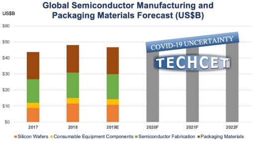
“From our market research, materials suppliers are increasing production and sales to ensure safety-stock throughout the supply-chain in case there are further disruptions due to COVID-19 cases,” remarked Lita Shon-Roy, TECHCET President and CEO. “Even without further disruptions, we can already see leading economic indicators such as unemployment levels, metal prices and container shipping indices point toward a significant decline in global GDP.” This is supported by the International Monetary Fund’s (IMF’s) current outlook on 2020.
Currently, almost all chip fabs appear to be running at normal levels, with a few exceptions. During this difficult period, YMTC in Wuhan, China reportedly has maintained R&D and grown production of 3D-NAND chips. However, chip fabs in Malaysia report that the government required companies to request permission to continue operating at 50% staffing levels. One company in France had to temporarily reduce production due to their labor union insisting on temporary workforce reductions.
Significant value-added engineered materials including specialty gases, deposition precursors, wet chemicals, chemical-mechanical planarization (CMP) slurries & pads, silicon wafers, PVD/sputtering targets, and photoresists & ancillary materials for lithography are reporting healthy orders and in some cases will see better than expected
revenues for 1Q2020 and April 2020. However, more than 60% of all materials are expected to be negatively impacted before year-end.
Overall demand for commodity materials, such as silane and phosphoric acid, is expected to decline YoY in 2020 by an average of 3% due to softening of the global economy. Average selling prices (ASP) for electronic-grade commodities may drop due to cost reductions in feed-stocks; for example, the global helium (He) gas market which
had been forecasted to be in shortage with high ASPs throughout 2020 has already improved due to COVID-19 slowing down helium demand.
DRAM, 3D-NAND, and MPU chips for server / cloud-computing applications are now in high demand for virtual meetings and remote work. It is yet unclear how much of an increase in materials shipments will be needed to support this segment, however from TECHCET’s modeling of prior cycles it will likely be >7%. Despite such an increase in
the materials used to make leading-edge ICs to build out data centers, shipments in support of legacy node IC fabrication are expected to decline this year.
Consequently, cloud-computing growth may not compensate for overall reduced semiconductor materials demands caused by economic downturns this year. By 2021 the global economy and all chip fabs should return to healthier growth, with materials markets for all IC devices expected to increase at a CAGR of +3.5% through 2025.
Critical Materials Reports™ and Market Briefings: TECHCET Shop
CMC Events: Click here to view all Events
EUV Materials Small But Strategic Fraction of $1.6B IC Photoresists Market
San Diego, CA, March 9, 2020: TECHCET announced that the global market for Photoresists and Ancillary Materials declined in 2019 due to semiconductor fabrication market challenges. However, growth is forecasted to resume this year, albeit limited by the COVID-19 drag on the global economy. G-Line/I-Line and DUV photoresists should exceed US$1.6 billion in 2020, as detailed in the latest Critical Materials Report™ (CMR) quarterly update on Photoresists & Ancillaries (see Figure). Meanwhile, the global market for extremely strategic EUV photoresists is expected to be just over US$10 million this year with a compound annual growth rate (CAGR) of over 50% through 2023.
“After many years of delays EUV is finally happening in IC fabrication, with advanced logic lines at Intel this year joining lines at Samsung and TSMC in using EUV, and ASML shipping a new stepper to SK hynix in the fourth quarter of 2019,” explained Ed Korczynski, TECHCET senior analyst and author of the report. “As a clear sign that EUV technology is now ready for commercial manufacturing, specialty EUV resist supplier Inpria just announced a $31 million Series C investment from a syndicate led by photoresist manufacturer and existing investor JSR Corporation.”
Inpria’s new investors included SK hynix Inc. and TSMC Partners. The round also includ-ed participation from existing investors Air Liquide Venture Capital ALIAD, Applied Ven-tures, Intel Capital, and Samsung Venture Investment Corporation.
ASML sold 203 DUV in 2019, and 26 EUV tools with 7 shipped in the third-quarter and 8 shipped in the fourth-quarter. The company claims capacity in 2020 to ship 30 NXE:3400 series steppers, and with anticipated assembly efficiency improvements should be able to ship 40-45 EUV tools per year starting in 2021.
This report covers the following suppliers: Avantor, BASF, Brewer Science, Dongjin Semichem, Dongwu Fine-Chem, DuPont (formerly Dow), Eastman Chemical, FujiFilm, JSR, Kempur, KMG (Cabot Microelectronics), Merck/EMD, Moses Lake Industries, Nissan Chemical, PhiChem, SACHEM, Shin-Etsu, Soulbrain, Sumitomo, Suntific, Tama Chemical, Tokyo Ohka Kogyo, and Versum.
Purchase Reports Here: TECHCET Shop
Materials eBlast – Wet Chemicals & Specialty Cleans 2020 Q1
TECHCET announced that Fluorite, needed for hydrofluoric acid (HF), prices in China have decrease by 9% over the last several months. The price situation is dynamic, with China regulators tightening environmental standards resulting in export restrictions and the need to import some raw materials, as detailed in TECHCET’s latest Wet Chemicals & Cleans Quarterly Market Update.
South Korea & Japan have de-Whitelisted each other, thus increasing requirements for exporting to each country. Consequently, South Korea has qualified non-Japan sources of HF gas (for wet chemicals): Befar in China, and Soulbrain and Ram Technology in South Korea.
Chemical specifications continue to change due to greater sensitivity of IC devices at the advanced nodes to impurities. To supply the most advanced fabs, chemical companies must be able to show a “fingerprint profile” of all chemical impurities.
Wet chemicals global market is forecasted to grow from approximately US$2.2B in 2019 to nearly US$2.9B by 2024, with a CAGR of 5.7%, as shown in the figure below:
More info Here
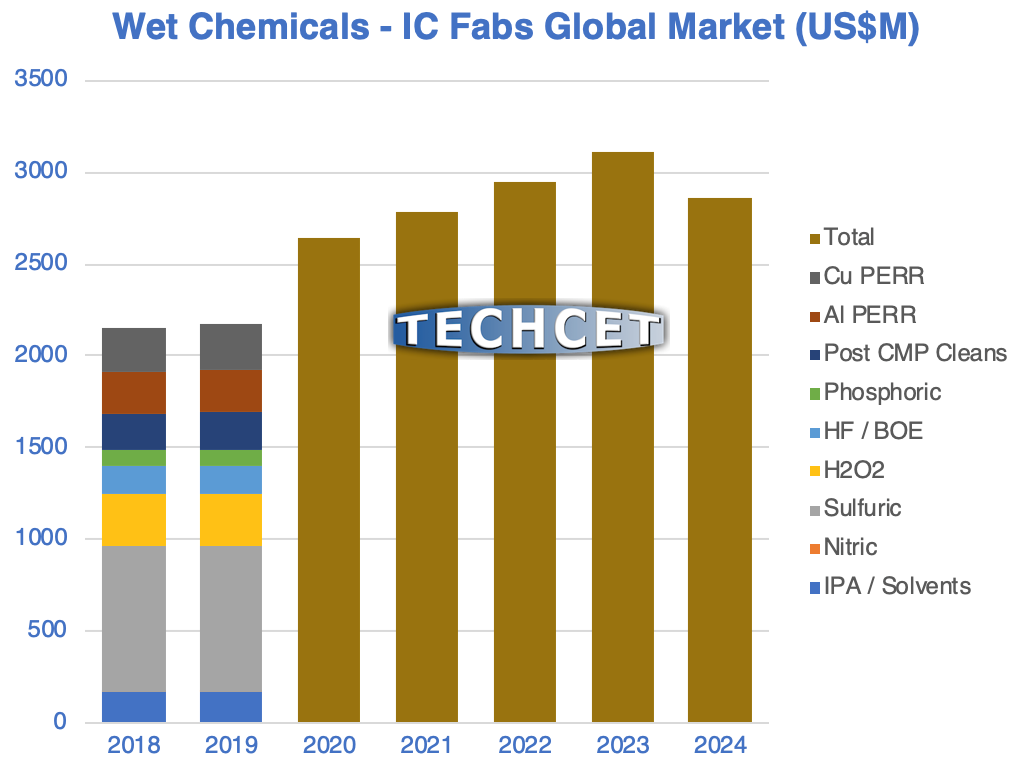
Semiconductor Materials growing to nearly $50B Market in 2020 after Downturn
San Diego, CA, January 14, 2020: TECHCET announced that global revenues for semiconductor manufacturing and packaging materials are expected to grow 5.7% year-over-year (YoY) in 2020 to US$49.5B, of which 65% represents semiconductor fab materials. The memory chip downturn in 2019 reduced total materials market revenues by 2.8% to US$46.8B in 2019, while the compound annual growth rate (CAGR) through 2023 is forecast at 3.5% as detailed in the latest TECHCET Critical Materials Reports (CMR) and shown in the attached figure.
“TECHCET sees the memory sub-market returning to growth in 2020, after the downturn that reduced semiconductor silicon wafer starts by more than 5% in 2019,” said Lita Shon-Roy, TECHCET President and CEO. “The production of semiconductor chips for modern communications, energy, healthcare, and transportation benefits the entire world, so we see steady growth in demand for semiconductor materials moving forward.”
At the 2020 Critical Materials Council (CMC) Seminar—held last October in Taoyuan, Taiwan—representatives of 14 global chip-makers including GlobalFoundries, Intel, Micron, Samsung, and TSMC discussed ways to ensure electronic materials supply-chain robustness in an era of short-sighted protectionist tariffs.
The public 2020 CMC Conference—happening April 23-24, 2020 in Hillsboro, Oregon—will follow private CMC meetings hosted by Intel that week. The keynote address on “Critical Materials Pushing the Limits for Semiconductor Manufacturing,” will be provided by Bruce Tufts, Vice President of Technology and Director of Fab Materials Organization, Intel. A new 4th Session on advanced packaging will highlight materials for chiplets in system-in-package (SiP) devices.
Critical Materials Reports™ and Market Briefings: TECHCET Shop
CMC Events: All CMC Events and Meetings
Cobalt and Nickel Targets Super Strategic for IC Fabs
San Diego, November 25, 2019: TECHCET announced that the global market for Physical Vapor Deposition (PVD) Sputter Targets is declining by 1.5% in response to semiconductor fabrication market challenges in 2019. However, 5% growth is forecasted for 2020, with the non-precious-metal segment expected to reach US$690 million. Including precious metals the 2020 Sputter Target market is expected to reach US$1,084 million, as detailed in the latest Critical Materials Report™ (CMR) quarterly update on Sputter Targets (see Figure).
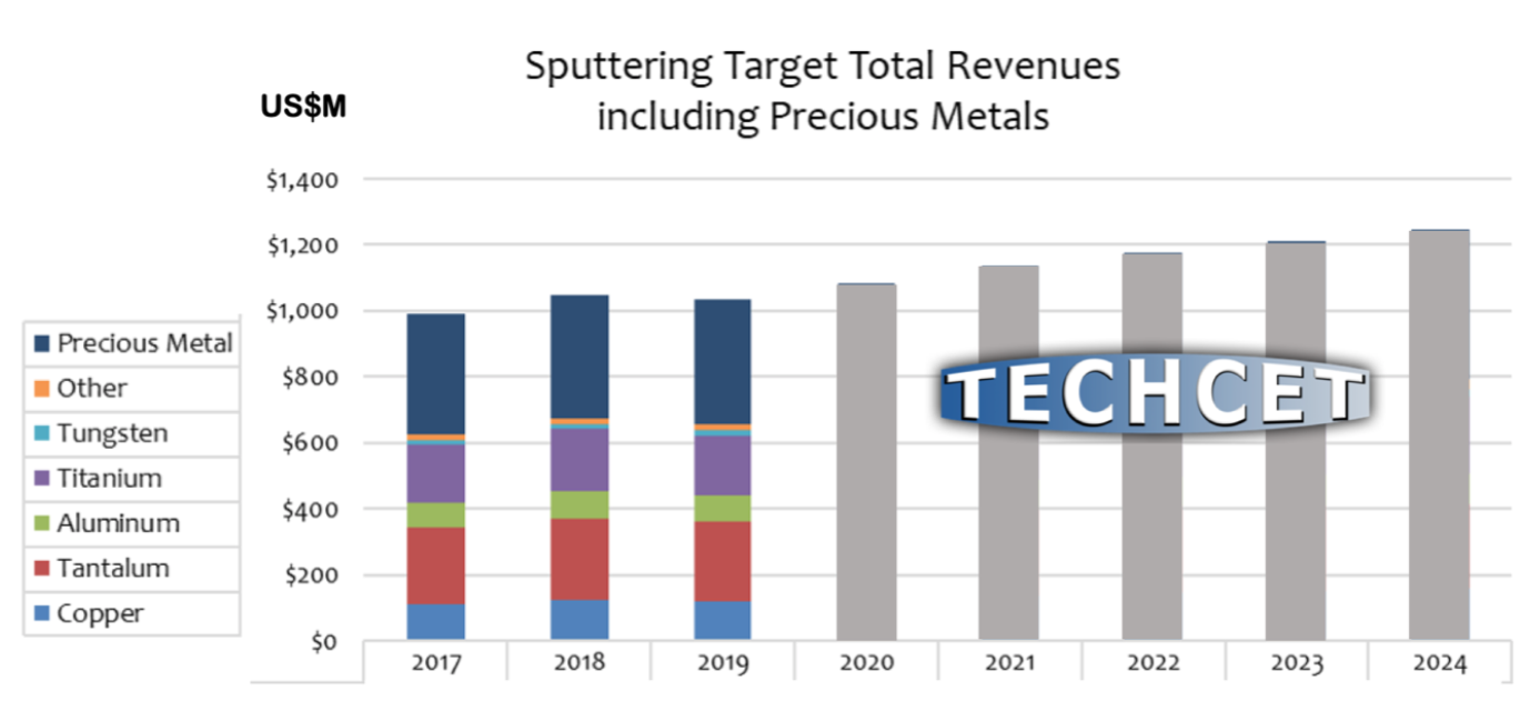
“Demand for ‘Other’ target metals such as nickel, cobalt, and multicomponent alloys are increasing,” explained Dr. Dan P. Tracy, TECHCET senior analyst and author of the report. “For emerging strategic applications, device makers may need to work with smaller, tier-2, suppliers, as their mainstay suppliers typically refrain from small volume
sub-markets.”
Overall, the Sputter Target manufacturing base is stable and keeping pace with industry. In the near term, TECHCET is tracking pricing trends for key metals such as tantalum and Platinum Group Metals (PGM).
This report covers the following suppliers: Furuya Metals, GO Element, Grikin, Honeywell, JX Nippon, KFMI, Materion, Pioneer Materials, Praxair/Linde, Sumitomo, Tanaka, Top Metal Materials, Tosoh SMD, Solar Applied Materials Technology, Umicore, VEM, and Vital Materials.
Purchase Reports Here: Sputter Targets
2020 CMC Conference & Call For Papers
San Diego, CA, November 21: The Critical Materials Council (CMC) of semiconductor fabricators and TECHCET announce a Call For Papers (CFP) to be presented at the 2020 CMC Conference, happening April 23-24 in Hillsboro, Oregon. As per the prior CMC Conferences (cmcfabs.org/cmc-conference-2020/), the 2020 event will explore actionable technical and supply-chain trends related to critical materials for global semiconductor fabs. Keynote address for this 5th CMC Conference will be:
“Critical Materials Pushing the Limits for Semiconductor Manufacturing”
Bruce Tufts, Vice President of Technology and Director of Fab Materials Organization, Intel Corp.
The conference committee is soliciting presentations on best practices of sourcing direct and indirect manufacturing materials for pilot lines and for high-volume manufacturing (HVM). Three sessions will cover the following themes:
I. Global value-chain issues of economics and regulations,
II. Immediate challenges of materials & manufacturing, and
III. Emerging materials in R&D and pilot fabrication.
CMC member companies will be attending the public CMC Conference, which follows the annual members-only CMC meeting to be sponsored by Intel and held April 21-22. Conference attendees will include industry experts handling supply-chains, business-development, R&D, and product management, as well as academics and analysts. Business drives our world, but technology enables the profitable business of manufacturing new devices in IC fabs, and new devices need new materials.
To submit a paper for consideration, please email us a 1-page abstract focusing on critical materials supply dynamics by January 15, 2020.
For more information on CMCFabs or CMC Associate Memberships, please contact Diane Scott. For information on sponsoring the CMC Conference please contact Yvonne Brown, +1-480-382-8336 x1.
Preventing Yield Losses a Key Topic of Critical Materials Council Meetings and Seminar
At the recently concluded TECHCET Critical Materials Council (CMC) Seminar in Taoyuan, Taiwan, a diverse gathering of industry experts discussed materials value-chain topics including quality issues, logistics best practices, and geopolitical disruptions. Seminar participants included individuals from device makers, material suppliers, and equipment and component providers from China, Europe, Japan, South Korea, Taiwan, and the U.S.
The keynote presentation by Mr. K. C. Hsu, Vice President of Micron Memory Taiwan, highlighted that, “data is today’s global currency,” and this is especially pertinent in high volume manufacturing (HVM). Data and information sharing along the materials supply-chain will allow semiconductor fabs to de-bottleneck supply and logistic issues. Early detection of materials quality and variability is critical to protect fab lines from yield excursions. As an example, Linde Electronics presented a thorough approach for de-bottlenecking the bulk specialty gas supply-chain from gas production through delivery to consumption in the fab.
As shown in The Figure, Ms. Jenny Tan, Sr. Manager for Global Procurement of Micron Technology, presented on “Challenges of Global Supply Chains” during the public CMC seminar. With HVM IC lines in the U.S., Japan, Singapore, and Taiwan to make commercial memory chips for the world, Micron Technology has to keep up the quality of critical materials sourced from both global and local suppliers. Seminar attendees also enjoyed presentations from Industrial Technology Research Institute (ITRI Taiwan), Pall Corp., United Silicon Innovation Corp., Air Liquide, ST Microelectronics, Lam Research Corp., and TECHCET analysts. Private discussions during coffee-breaks allowed attendees to network with industry experts.
Private Face-to-Face Meetings
Hosted by Micron Taiwan, the 2019 Fall CMC Fab Members private meeting occurred October 15-16. In addition to materials suppliers, representatives of the following semiconductor fabs attended this powerful meeting: Broadcom, Cypress, GlobalFoundries, Infineon, Intel, Micron, Nexperia, OnSemiconductor, Samsung, Sony, ST Microelectronics, TSMC, Texas Instruments, and TowerJazz Panasonic.
Topics discussed included trends influencing helium pricing, timely notification of materials end-of-life, and best practice to support growth of new suppliers. Fabs need more insights into sub-tier suppliers to avoid disruption and quality issues, and they typically do not talk directly with sub-tiers but expect direct suppliers to be in charge of communications. CMC members are seeing new Chinese suppliers approaching fabs directly, and this is an opportunity to develop improved protocols for assessing risk.
The afternoon of October 16th featured a joint session with Fab members and Supplier members talking about “The Hidden Cost of Supply Chain Disruption.” Much of the discussion in this session circled around the current geopolitical environment adding uncertainty and instability to the already stressed supply-chain. While trade disputes rage between national governments with no end in sight, commercial semiconductor fabs must keep shipping chips to keep our modern world working.
CVD SiC Strong Amid Weak Demand for Structural Ceramics in OEM Tools in Downturn
San Diego, CA, October 17, 2019: TECHCET—the advisory services firm providing electronic materials information— announced that the 2019 global market is softening for structural ceramics components needed in semiconductor Original Equipment Manufacturer (OEM) tools. Reports of ~ 15% year-over-year (YoY) drop in OEM tool sales are somewhat balanced by ceramic components growth in parts of Asia being net positive in 2019, so overall world-wide ceramic components sales are forecasted to be US$1.37 billion in 2019, which is just -5% YoY. A slow recovery is expected in 2020 leading to a forecasted ~4% compound annual growth rate (CAGR) over 2018-2023.
The highlights of the structural ceramics market include CVD silicon-carbide (SiC) and High Purity Alumina (HPA) parts. In particular, CVD SiC sales are supported by the trend of replacing quartz and alumina in the most advanced process chambers. CVD SiC is expected to grow >4% per year through 2023, and it is possible that >50% of SiC parts will be using CVD SiC in some form, including SiC:Graphite composites and CVDSiC on SiC components. Many components suppliers serve this market, although the top 3 companies in the lead remain Tokai Carbon, CoorsTek, and Asahi Glass (see Figure).
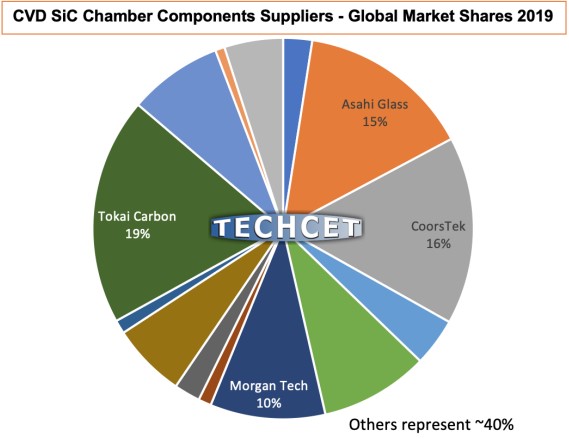
This report covers the following suppliers: ADMAP, Applied Ceramics, Asahi Glass, Bridgestone, Carborundum, Ceredyne/3M, CoorsTek Semiconductor Equipment Component, CoorsTek-Saint Gobain, CoorsTek, DuPont, Entergis, Ferrotec, Hitachi Chemical, Kyocera, Maruwa, Mersen, Morgan Technical Ceramics, NGK/NTK, SGL Group, Solmics, Toyo Tanso, Tokai Carbon Korea, Tokuyama, USTC, Worldex, Xycarb Ceramics, and more!
Purchase Reports Here: TECHCET Reports
Chinese and Korean Materials Suppliers Profiting from Japanese Politics
San Diego, CA, October 10, 2019: TECHCET—the advisory services firm providing electronic materials information—announced that Chinese materials suppliers are moving to take marketshare at South Korean chip fabrication (fab) lines. Due to residual animosity from 20th century wars, Japanese politicians decided to use the semiconductor materials supplier-chain as a pawn in a political chess game and un-white-listed South Korea from exports. Any good-will between the two nations was immediately erased, and South Korea announced a US$6B government investment to as a huge driving force to help develop local supplies. Now Chinese chemical suppliers have unprecedented openings to qualifications at Korean-owned fabs, including commercial memory fabs in China.
According to the official July 16 announcement of China’s New Materials Industry Alliance of Electronics and Chemical Industry, Befar Group’s electronic hydrofluoric acid has successfully received batch orders from some Korean semiconductor manufacturers. After many batches of sample testing and small batch testing, Befar Group finally established a formal partnership with Korean enterprises. Then on September 3rd, South Korea’s Yonhap news agency reported that according to an “informed official” Samsung Electronics has begun replacing HF sourced from Japan with critical material from local suppliers.”
“New sources of HF for high-volume manufacturing of semiconductors must be qualified though extensive split-lot experiments to ensure that there will be no yield losses,” reminded Lita ShonRoy, President and co-founder of TECHCET. “Our industry sources indicate that qualifications of Chinese chemical suppliers, like Befar, is of high interest to Korean chip fabricators. Now the door is open, and Chinese suppliers are on the ready to get qualified by South Korean electronics manufacturers, especially at Samsung Xian and SK hynix Wuxi.”
Fluorspar mineral is the raw material source for HF, and most (~60%) of the world’s fluorspar is mined in China and to a lesser degree (< 20%) from Mongolia. Fluorspar supplies remain tight worldwide with much of Mongolia’s 2019 production having already been sold into Chinese and other Asian markets, with continuing strong demand from these markets and good prospects for additional sales. Over the past year, supply-chains outside of China have tried to qualify local fluorspar sources, but the Asian region will remain very dependent on China for this important mineral and for fluorinated gases.
TECHCET is tracking the following Chinese materials suppliers: Anji Microelectronics Co.,, Befar Group Co., Grikin, Guangdong Huate Gas Co., Hefei TNJ Chemical Industry Co., Hubei Feilihua Quartz Glass Co., Jiangsu Denoir Technology Co., Jiangyin Jianghua Microelectronics Materials Co., Kempur Microelectronics, Konfoong Materials International Co. (KFMI), Linggas dba Green Link Electronic Materials Co., Rudong Zhenfeng Yiyang Chemical Co., Shanghai Phichem Material Co., Shanghai Sinyang Semiconductor Materials Co., Suzhou Ruihong Electronic Chemicals Co., Yingde Gases Group Co., Zhangjiagang Free Trade Zone Monheit International Trade Co., and Zhejiang Yongtai Technology Co.
Purchase Reports Here: https://techcet.com/product/china-briefing/
Global Market Remains Strong for ALD & CVD Precursors in IC Fabs
San Diego, CA, October 2, 2019: TECHCET—the advisory services firm providing electronic materials information— announced that the global market for atomic layerdeposition (ALD) and chemical vapor deposition (CVD) precursors is showing strong growth despite semiconductor fabrication market challenges in 2019. CVD growth is mainly in plasma-enhanced CVD (PECVD) and metal-organic CVD (MOCVD) for silicon ICs and for newer devices including micro-displays, RF for 5G, and photonics. The combined ALD and CVD metal precursor market is estimated to be approximately US$582M in 2019 growing 6.3% from the prior year and forecasted to grow above US$930M by 2025, as detailed in the latest Critical Materials Report™ (CMR) on ALD / High-K Metal Precursors (see Figure).
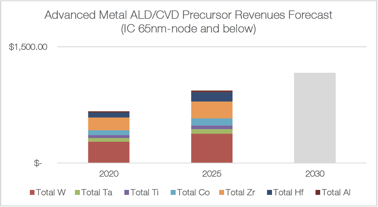
“Today, the top three suppliers ADEKA, Air Liquide, and Versum dominate the market by controlling ~75% of the segments,” explained Dr. Jonas Sundqvist, TECHCET senior technology analyst and author of the report. “However, due to the recent development that Merck will acquire Versum, there is a good chance that by doing so it will become the number one supplier for all type of metal, High-κ, and dielectric precursors.” The CVD, ALD, and SOD market includes from both specialty gases (e.g. WF6) and liquid precursors, as well as a considerable segment of solid precursors (e.g. HfCl4, PDMAT). In addition, there are smaller segments for precursors that still do not reach annual sales of >US$5 million such as ruthenium and rare earth elements (REE).
This report covers the following suppliers: ADEKA, Air Liquide, Air Products, AZmax Co., BASF, DNF Co., Entegris, Epivalence, FujiFilm, Gelest, Hansol Chemical, H.C.Starck, Kojundo, Linde (Praxair), Mecaro, Merck EMD, Nanmat, Norquay, Pegasus Chemicals, Soulbrain, Strem, Tanaka Kikinzoku Group, Tokyo Chemical Industry Co.,Tri Chemical Laboratories, Umicore, UP Chemical (Yoke), and Versum.
Purchase ALD/CVD Reports Here: TECHCET Reports
Fab Materials Resilient Despite 2019 Downturn
2020 Expected to Resume Steady Growth
San Diego, CA, September 10, 2019: TECHCET—the electronic materials advisory services firm providing business and technology information— forecasts that global trade wars have reduced downstream demand for semiconductors although semiconductor fabrication (fab) materials markets will shrink only slightly in 2019. In April of this year TECHCET had forecast growth of ~3.0%, while the updated forecast shows a shrinking of ~1.4% total market in the global market for semiconductor manufacturing materials to reach a total of over US$47 billion (see Figure). The forecasted compound annual growth rate (CAGR) through the year 2023 has correspondingly been reduced from 4.3% to 3.6% in anticipation of reduced steady growth.
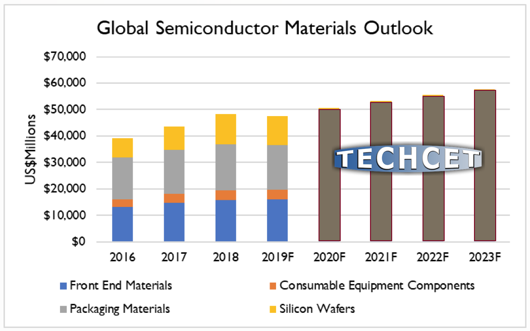
Dr. Dan P. Tracy, Director of Market Research & Sr. Analyst of TECHCET, provided this update on the global semiconductor manufacturing materials market on September 10th at the 2019 China Semiconductor Materials Innovation and Development Conference sponsored by China’s Integrated Circuit Materials & Components Industry Technology Innovative Alliance (ICMtia). Tracy’s presentation on “Materials Challenges and Opportunities for Emerging Device Applications” covered the updated TECHCET materials outlook and discussed trends in device scaling which provide opportunities for material suppliers.
“Advanced technology chip fabs are driving higher than originally expected growth of traditional wet chemicals for cleaning because of two technology shifts,” explained Tracy. “First there is increased adaption of single-wafer spray tools that use more chemistry than conventional batch tools, and second there are more multi-step wet clean processes needed for surface treatment and residue removal. Consequently, TECHCET is forecasting greater than 5% CAGR over the period 2018-2023 for wet chemicals.”
Dynamics of localization within the global supply-chain will be discussed at the 4th annual public CMC Seminar, happening October 17 in Taoyuan, Taiwan. Attendees will gain insights on challenges associated with supplying quality materials, local government initiatives, and globalization trends which support the rapidly growing supply-chain within Greater China and Asia at large. Attendees have the opportunity to network with CMC Fab members who will have just finished their private face-to-face meetings held earlier that week.
Critical Materials Reports and market briefings: TECHCET Reports
CMC Seminar: CMC Seminar 2019
4th CMC Seminar Focus on Materials Quality
Quality Excursions Can Cost Fabs Hundreds of Millions of Dollars
The Critical Materials Council (CMC), a unit of TECHCET, announces that their 4th annual public CMC Seminar will be focused on quality excursions and the global materials value-chain. Fabs such as local Taiwanese powerhouse TSMC have suffered millions of dollars in lost product revenues due to quality excursions in materials from global materials suppliers. The CMC Seminar is one of the best forums to learn about these challenges and opportunities related to evolving electronic materials supply-chains.
The CMC Seminar explores the dynamics of local materials supply-chains within global markets. Along with a panel discussion between invited CMC fabs and material suppliers and networking opportunities, there will be timely presentations on the following topics:
• Keynote on “Navigating Global and Local Semiconductor Materials Markets and Supply-Chains,” presented by Mr. KC Hsu, Vice President of Micron Memory Taiwan,
• “Bulk Specialty Gas Supply: Debottlenecking the Electronics Material Supply Chain From Material Production to Fab Consumption,” by Dr. Hok Tsan Lam, Head of Business Development for
Linde Electronics,
• “Solving Challenges in Vapor Concentration Delivery,” by Mr. Ray Morgan, Director of Veeco,
• “Prevention & Control of Particles & Heavy Metal Contamination in Fabs,” by Dr. David Huang, Vice President of Pall Filters,
• “Global Materials Markets and Forecasts,” by Dr. Dan Tracy, Sr. Analyst of TECHCET, and
• “Challenges of Global Supply Chains,” by Ms. Jenny Tan, Sr. Manager for Global Procurement of Micron.
Attendees will have opportunities to network with CMC Fab members who will have just finished their private face-to-face meetings held earlier that week.
Who Should Attend?
I. Semiconductor device fabricators,
II. Materials and equipment suppliers, and
III. Financial analysts, with an interest in semiconductor process materials markets.
For more information and to register for the event: CMC Seminar 2019
CMC Fab members include:

Micron VP Keynote for the 4th CMC Seminar
Event in Taiwan 17 October will feature a keynote from Micron Technologies
The Critical Materials Council (CMC) of semiconductor fabricators is pleased to announce that the keynote presentation for the 2019 CMC Seminar will be “Navigating Global and Local Semiconductor Materials Markets and Supply-Chains,” presented by Mr. KC Hsu, Vice President of Micron Memory Taiwan. The public CMC Seminar will be held on October 17th at the Fullon Hotel A8 in Taoyuan, Taiwan. Attendees have the opportunity to network with CMC Fab members who will have just finished their private face-to-face meetings held earlier that week.
The CMC Seminar focuses on the dynamics of local materials supply-chains within global markets. Global fabs and suppliers are increasingly challenged in managing materials requirements, quality control, and logistics issues across many regions. The CMC Seminar is one of the best forums to get information on the rapidly growing electronic materials supply-chain within Greater China and Asia at large.
Who Should Attend?
I. Semiconductor device fabricators,
II. Materials and equipment suppliers, and
III. Financial analysts, with an interest in semiconductor process materials markets.
For more information and to register for the event: Please Click here
Quartz Revenues a Positive Sign Amidst Equipment Sales Declines
San Diego, CA, August 06, 2019: TECHCET—the advisory services firm providing electronic materials information—announced that the global market for quartz equipment consumables used in semiconductor manufacturing is forecasted to drop only -3% this year to US$1.26 billion for fabricated parts and $425M for base materials. These moderate decline estimates are attributed to current long lead-times and lean parts inventories; both positive signs amidst the negative growth (<-15%) of the OEM equipment market expected for 2019. Despite this year’s forecast, the 5-year compound annual growth rate (CAGR) for both base materials and fabricated parts is estimated to be approximately 5% over the period 2018-2023, as detailed in the latest Critical Materials Report™ (CMR) on Quartz Materials (see Figure)
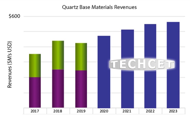
“A major 2019 theme in the quartz industry serving semiconductor manufacturers is consolidation through mergers and acquisitions,” explained Kuang-Han Ke, TECHCET senior technology analyst and author of the report. “Companies in this sector seek to become more vertically integrated up and down the supply-chain, with fabricators and base materials suppliers merging, and powder suppliers facing internal restructuring.”
Supply of 300mm quartz tubes for diffusion furnaces is limited in 2019 by the need for experienced workers, which faces a lag in development. Supply of machined parts can be increased more easily due to less need for skilled labor. Some portions of the market, especially DRAM and NAND memory fabs, will be affected more than others in 2019.
This report covers the following suppliers: Applied Ceramics, Beijing Kaide, DS Techno, Donghai Baosheng Quartz Products Co., Ferro Tec, GM Associates, Hangzhou Dahe Thermo-magnetics Co., Hanntek, HanYung, Hayward Quartz Technology, Hongwei Quartz, Hsin Yui Technology Co., Heraeus Quarzglas, Hubei Feilihua Quartz Glass Co., Huzhou DongKe, Japan Super Quartz, Jiangsu Pacific Quartz Co., Jinzhou East Quartz, Jinzhou New Century Quartz, Kumkang Quartz (KKQ), Maruwa Quartz, Momentive Performance Materials, Quartz(GE), Quality Quartz Engineering, Quick Gem Optoelectronic S & T Co., Shanghai Qianghua Quartz Co., Polar Quartz, QSIL, Russian Quartz, Shin-Etsu Quartz/Heraeus-Shin-Etsu Quartz Products (HSQP), SungRim, Taicang Huaan Quartz Glass Product Co., Techno Quartz, Tosoh Quartz, The QUARTZ Corp., Topco / Heraeus in Taiwan, Unimin, Wonik QnC, Worldex/West Coast Quartz, XingHu Shanghai, Xycarb Ceramics, Young Shin.
Purchase Quartz Reports Here: TECHCET Reports
Litho Materials Market Growing to $3.2B in 2019 Despite Trade Wars
San Diego, CA, July 22, 2019: TECHCET—the advisory services firm providing electronic materials information— announced that the global market for lithography materials in semiconductor manufacturing is forecasted to grow to US$3.2 billion in 2019 despite ongoing trade wars. As of July 4, Japan imposed export restrictions on three key materials purchased by S. Korea, including advanced photoresists, materials critical for semiconductor manufacturing. Trade tensions between the two countries are causing ripples in the supply-chain as companies try to mitigate any possible availability issues. At present, the latest Critical Materials Report™ (CMR) on Photoresists, Extensions, and Ancillary Materials, shows 2019 global sub-market sizes of US$1.7 billion, US$0.9 billion, and US$580 million (respectively). Despite these trade issues, TECHCET sees steadily increasing demand for litho materials to reach approximately US$4B in 2023 (see Figure).
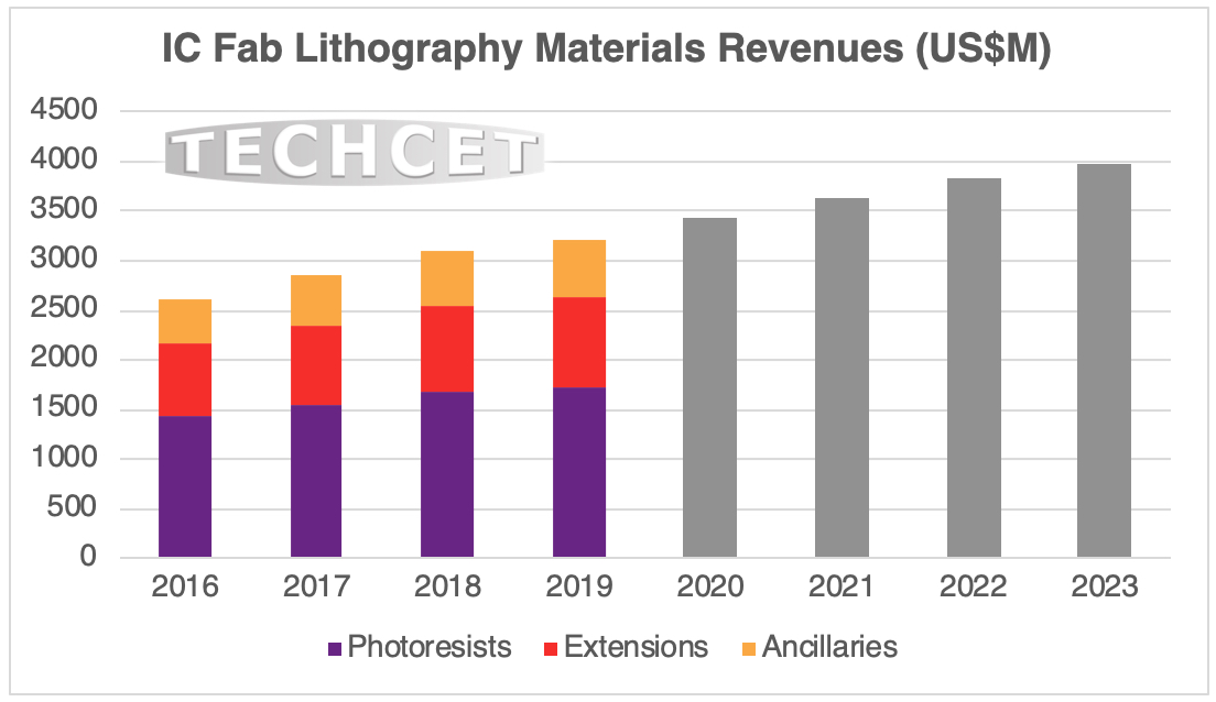
TECHCET sees steadily increasing demand for lithography materials
“EUV lithography is first being used by Samsung Electronics to reduce turn-around-time and improve yield in their 7nm-node logic line in South Korea, while the designs allow for multiple exposures of 193nm DUV lithography to produce the same chips in more time,” explained Ed Korczynski, TECHCET senior technology analyst and author of the report. “However, qualifying a new IC lithography material for high-volume manufacturing typically takes many months and millions of dollars in test wafers and metrology, so the recent export restrictions by Japan will definitely hurt the bottom lines of South Korean fabs.”
DUV and EUV photoresists are highly engineered chemical blends which cannot be easily replicated, so it is unlikely that South Korean chemical companies can establish local production by 2020. TECHCET estimates that the Top-6 photoresist suppliers represent >85% of the global market, and of those only DuPont is not a Japanese company. Consequently, the action by the Japanese government to restrict Japanese photoresist sales to South Korea represents a gift of market share to DuPont.
This report covers the following suppliers: Avantor, BASF, Brewer Science, Dongjin Semichem, Dongwu Fine-Chem, DuPont (formerly Dow), Eastman Chemical, FujiFilm, JSR, Kempur, KMG (Cabot Microelectronics), Merck/EMD, Moses Lake Industries, Nissan Chemical, PhiChem, SACHEM, Shin-Etsu, Sumitomo, Suntific, Tama Chemical, Tokyo Ohka Kogyo, and Versum.
Purchase Photoresists Reports Here: TECHCET Reports
CMP Materials Market Reaches $2.7B Amid Signs of Orders Slowing in 2019
San Diego, CA, June 19, 2019: TECHCET—the advisory services firm providing electronic materials information— announced that the global market for chemical-mechanical planarization (CMP) consumable materials in semiconductor manufacturing is forecasted to grow to US$2.7 billion in 2019. However, several suppliers report softening orders for the first half of 2019 due to shifting wafer starts combined with intensified industry efforts to save slurry costs through increasing dilution. There is also substantial uncertainty in the slurry supply-chain due to China’s dominance of ceria refining. The latest quarterly update to the Critical Materials Report™ (CMR) on CMP Slurry, Pads, and Conditioners, shows global sub-market sizes of US$1.4 billion, US$1.0 billion, and US$300 million (respectively).
“Colloidal ceria nano-particles have long been established as the preferred abrasive for CMP slurries for shallow trench isolation and other specialty planarization processes in device manufacturing,” explained Dr. Diane Scott, TECHCET senior analyst and coauthor of the report along with Dr. Rob Rhoades. “However, recent threats to the ceria supply-chain from China are leading many fabs to begin qualifying alternative slurries to reduce the risks of either dramatic cost increases or production disruptions.”
Increased use of 3D structures in leading edge digital ICs leads to the need for more CMP process steps in their fabrication. Advanced process integrations are also driving increased customization of consumable materials to achieve the necessary planarization at each level. Consequently, the market growth for CMP consumables should outpace the market growth for silicon wafers in IC fabs.
This report covers 58 supplier profiles: 3M, Ace Nanochem, Adcon Lab, Anii Microelectronics, Asahi Glass, BASF, Bailkowski/PSB, Cabot, Dongjin SemiChem, DowDupont, Eka Chemical/Akzo Nobel, Eikem, Eminess Technologies, Evonik Industries,Ehwa, Ferro, FujiFilm, Fujimi, Fuso Chemical, General Engineering and Research, W.R.Grace, Hitachi Chemical, Innovative Organics, Intersurface Dynamics, JGC C&C, JSR, KC Tech, Kemesys, Kinik, Merck (incl. former AZ Chemical), Mitsui Mining & Smelting, Morgan Advanced Ceramics, Nalco, Nano Phase Technologies, Nissan Chemical Industries, Nitta-Haas, Precision Colloids, Rhodia (Solvay), Samsung (Cheil Industries), Showa Denko, Sibond, Saint-Gobain, Soulbrain, UK Abrasives, U Wiz Technology, Universal Photonics, Versum, and Wacker Chemie.
Purchase CMP Reports Here: TECHCET Reports
4th CMC Conference Enabled Critical Information and Connections
Event in Albany area 25-26 April featured GlobalFoundries keynote and presentations
May 7, 2019 – San Diego, CA
 Over 150 leading executives and managers within the semiconductor manufacturing ecosystem gathered on April 25th and 26th in the Albany area of New York state for an important event on fabrication (fab) materials. The fourth-annual Critical Materials Council (CMC) Conference, produced by TECHCET, included topical presentations, a fab tour, exhibits by specialty materials suppliers, and networking roundtable discussions to learn about best-practices in a pre-competitive environment. Folks who missed attending the event this year can register to access the posted presentations for a nominal fee at our CMC Fabs Website. Please click here to get more info.
The event opened again, as in each of the prior three years, on an extremely strong business and technology keynote address by an executive from one of the CMC Fab member companies. The 2019 CMC Conference keynote was given by Dr. John Pellerin, Deputy CTO and VP of Worldwide R&D, GLOBALFOUNDRIES. Pellerin talked about how demand for new high-volume manufacturing (HVM) semiconductor devices over the next few years will drive needs for increased numbers of new specialty materials as well as volumes of existing materials in his presentation on “Materials Challenges & Opportunities in Differentiated Technologies.”
In the first session of the event covering global supply-chain issues of economics and regulations, G. Dan Hutcheson, CEO of VLSI Research, presented on “Slowdown: When did it start? What drove it? And When will the recovery come?” Hutcheson showed data from leading economic indicators that the recent decline in global semiconductor fab industry revenues due to memory chip prices may have already turned around.
TECHCET Sr. Analysts Dr. Jonas Sundqvist and Terry Francis presented updated information on demand drivers and forecasts for ALD/CVD precursors and Rare Earths, respectively. Sundqvist–also leader of the Thin Film Technologies Group at Fraunhofer IKTS–focused on how new 3D memory and logic chips demand more deposition precursors such that chemical volume growth will outpace that of silicon wafers, shown in the Figure. Francis showed how “Rare Earth” elements are not so rare at the elemental level, but complex dynamics between mining and refining and capitalism have led to a situation where mainland China currently controls most of the market for elements such as lanthanum (used in advanced ICs to create CMOS logic gates). Deep dives into all such materials matters are found in the TECHCET Critical Materials Reports (CMR), and you can find all of them online at TECHCET Shop.
The 2020 spring CMC Conference is scheduled for April 24-25 in Austin, Texas. Austin is home to CMC Fab members Cypress and Samsung Austin Semiconductor (SAS). The CMC Fab members and Associate members will again gather for two days of private face-to-face meetings before attending the public CMC Conference. In addition to the annual spring CMC Conference in the US, there is also an annual fall CMC Seminar in Asia. The 2019 CMC Seminar will be held on October 17 in Taoyuan, Taiwan. For more information on CMC events see TECHCET Events
China Fab Materials Trade Facing Uncertainty
Tariffs and Supply-Chains discussed at SEMICON China
San Diego, CA, April 3, 2019:
TECHCET—the electronic materials advisory services firm providing business and technology information— announced that uncertainties in global trade have created both rising and falling fortunes for China’s semiconductor fabrication materials industry. China’s exports are slowing compared to 4Q2018, especially for companies supplying to Japan, Korea, and Taiwan. However, material companies supplying into Europe have seen healthy bookings this quarter. In addition, companies providing materials consumed in power devices report that business remains positive. TECHCET forecasts growth of ~3 percent this year in the global market for semiconductor manufacturing materials to reach a total of just over US$50 billion.
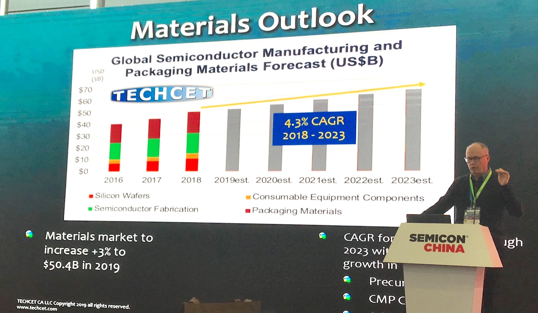
Dr. Dan P. Tracy, Director of Market Research & Sr. Analyst of TECHCET, recently provided an update on the global semiconductor manufacturing materials market at the 2019 SEMICON China conference. He discussed the materials driving steady demand increases at 4.3 percent compound annual growth rate (CAGR) through the year 2023, as shown in The Figure. There is an expectation for business to improve in general in 2H2019 as supply:demand returns to balance in the current memory-cycle.
SEMICON China is now the largest semiconductor equipment and materials trade show in the world. The show was packed overflowing into multiple tent areas because there was not enough room in the regular expo halls. Equipment and materials companies from all over the world were represented, with a strong showing of Chinese suppliers.
Local environmental regulations on mining and refining continue to be enforced with more stringent curtailment of those with no government affiliation. Larger companies with more capital to invest in regulation compliance are still in operation. Chinese companies well positioned to reap the benefits of vertically integrated supply-chain include 718/Peric as the largest ammonia and specialty-gas maker with direct investment in fluorspar mines, and Xingfa Group the largest phosphoric acid maker whose majority owner also owns phosphor rock mines. Dynamics of the global supply-chain will be discussed at the 4th annual CMC Conference, happening April 25-26 in Saratoga Springs, NY. Details of fab materials forecasts are found in TECHCET’s extensive Critical Materials Reports™.
Critical Materials Reports™ and market briefings: Please click here
CMC Conference: Please click here
ABOUT TECHCET: TECHCET CA LLC is an advisory services firm focused on process materials supply-chains, electronic materials business, and materials market analysis for the semiconductor, display, solar/PV, and LED industries. Since 2000, the company has been responsible for producing the SEMATECH Critical Material Reports™, covering silicon wafers, semiconductor gases, wet chemicals, CMP consumables, Photoresists, and ALD/CVD Precursors. The Critical Materials Council (CMC) of semiconductor fabricators is a business unit of TECHCET, and includes materials supplier Associate Members. For additional information about reports, market briefings, CMC membership, or custom consulting please contact [email protected], +1-480-332-8336, or go to www.techcet.com or www.cmcfabs.org
Critical Materials Business and Technology Information 2019
4th Annual Critical Materials Council (CMC) Conference April 25-26 in Saratoga Springs, New York. – A must-attend for business and technology professionals concerned with global supply-chains for semiconductor manufacturing.

2019 Critical Materials Council(CMC) Conference Sponsors
TECHCET will host the 4th annual Critical Materials Council (CMC) Conference April 25-26 at the Saratoga Hotel and Casino in Saratoga Springs, New York. At the CMC Conference, business visionaries and manufacturing technologists gather to address current and future maaterials challenges. The latest forecasts on market drivers including trade issues, along with technical issues facing the global materials supply-chain, will be shown.
The public CMC Conference follows private CMC face-to-face meetings to be held April 23-24, 2019 at GlobalFoundries in Malta, New York. Themes are centered around the needs of the Critical Materials Council and the global IC fabrication industry. While executive conferences typically focus on the “what” and “why” of materials technologies, this conference will discuss “how” new materials can be controllably, safely, and cost-effectively used in fabs.
The CMC Conference this year will feature a keynote presentation on “International Supply-Chain Management Challenges,” by Dr. John Pellerin, Deputy CTO and VP of Worldwide R&D of GlobalFoundries.
Other featured presentations include:
• Tim Yeakley, ESH Policy Manager, Texas Instruments, on “Global Materials Regulation Issues,”
• Dr. Karl Robinson, Director of Process Engineering, IMEC, on “Materials Engineering in CMOS and Beyond-CMOS Applications,”
• Dr. Bryan Rice, VP of Product Integration, Inpria Corp., on “EUV Photolithography Materials Integration,”
• G. Dan Hutcheson, CEO, VLSI Research, on “Slowdown: When did it start? What drove it? and When will the recovery come?”
• Gus Richard, Managing Director, Northland Securities, on “Macroeconomics & Drivers Influencing the Electronics Industry.”
Attendees from fabs, OEMs, and materials suppliers alike will have the opportunity to interact with the presenters and colleagues, to gain insights into best-practices of the entire supply-chain.
Register now at the early-bird rate of just $395: https://cmcfabs.org/cmc-events/
Semiconductor Materials Market will be +3% to $50.4B in 2019
TECHCET’s Forecast Remains Strong Despite Trade Wars
San Diego, CA, January 9, 2019:
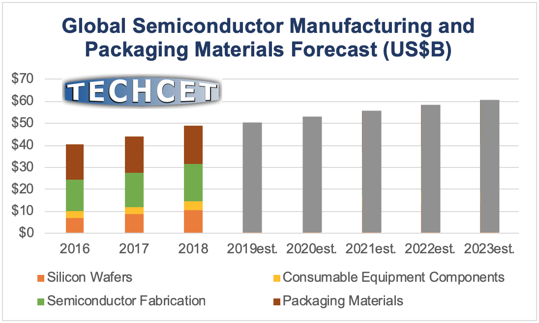
TECHCET—the electronic materials advisory services firm providing business and technology information— announced that global revenues for semiconductor manufacturing and packaging materials are expected to grow 3.1% year-over-year (YoY) in 2019 to US$50.4B, of which 58% represents semiconductor fab materials. Steadily increasing demand for memory chips in 2018 lifted total materials market revenues to US$48.9B in 2018, while the compound annual growth rate (CAGR) through 2023 is forecast at 4.3% as detailed in the latest TECHCET Critical Materials Reports (CMR) and shown in the attached figure.

Global trade issues in 2018 run the risk of devolving into real trade wars, if governments and companies do not negotiate business terms from a place of mutual respect. “Wars can only have winners and losers,” reminded Lita Shon-Roy, TECHCET President and CEO. “While issues can have win-win resolutions after mutually respectful negotiations.”
At the 2018 Critical Materials Council (CMC) Seminar, held last October in Ningbo, China in coordination with China’s IC Materials Technology Innovation Alliance (ICMtia), representatives of global chip-makers including Intel, GlobalFoundries, and Texas Instruments discussed ways to ensure electronic materials supply-chain robustness in an era of short-sighted protectionist tariffs. All three companies have high-volume manufacturing (HVM) fabs in mainland China along with the US and all need to source a wide range of specialty materials from global suppliers.
During private face-to-face meetings between CMC fab members in Ningbo, held just after the public CMC Seminar, companies shared that they have plans prepared to deal with tariffs goings into effect at different levels. Established HVM chip fabs must keep sourcing specialty materials regardless of political whims because our modern world relies on a steady supply of semiconductor devices to maintain our communications, entertainment, health-care, and transportation infrastructures.
Critical Materials Reports™ and Market Briefings on: Techcet Shop
For additional information about these reports or CMC Fabs membership please contact Diane Scott at [email protected] +1-480-332-8336, or go to www.techcet.com or www.cmcfabs.org.
IC Lithography Materials Market at $6.8B by 2023
EUV lithography demand small but strategic
San Diego, CA, September 28, 2018: TECHCET—the advisory services firm providing electronic materials information— announced that global IC fabrication demand for photoresists and ancillary lithography materials is growing strongly from an estimated market size of US$5.2 billion in 2017 to US$6.8 billion in 2023. Demand for argon-fluoride immersion (ArFi) photoresists is now growing at nearly 10 percent by volume. Extreme Ultra-Violet (EUV) lithography will soon be entering limited production use at Samsung and TSMC, with Intel and other companies expected to follow use after this year. However, the total market for EUV photoresists in the year 2023 is forecast to be just US$100 million, as detailed in the latest TECHCET Critical Materials Report (CMR) on photoresists and ancillaries.
“EUV is finally happening but the total market for resists next year is forecast to be only 8 million dollars,” said Ed Korczynski, TECHCET senior analyst and author of the report. “Our proprietary cost-models show that EUV can be cost-effective when the proper materials are integrated, and that resolution-extension materials such as anti-reflective coatings and shrink/trim materials add tremendous value to microlithography in general and to EUV litho in particular. When a single EUV stepper costs 120 million dollars and exposes 10 million wafers before wearing out, the CapEx depreciation per wafer is 12 dollars. In comparison, a high-value-add litho material may cost just 1 to 2 dollars per wafer to significantly improve the speed or resolution of the patterning.”
One significant change in the regulatory landscape is increasing restrictions on the use of N-methyl-2-pyrrolidone (NMP) as a solvent in microlithography. NMP has been widely used in other industries and toxic residues can remain in consumer products, so the material is now on the U.S. EPA’s Top10 list of priorities for regulation in 2019. Suppliers are working with fabs to find a less-toxic solvent to replace NMP.
Suppliers covered in this report include: Avantor, Brewer Science, Chang Chun, Dongwu Fine-Chem, DowDuPont, Eastman Chemical, FujiFilm, JSR, Kempur, KMG (Cabot Microelectronics), Merck/EMD, Moses Lake Industries, Nissan Chemical, SACHEM, Shin-Etsu, Sumitomo, Tama Chemical, and Tokyo Ohka Kogyo.
Purchase Reports Here: Photoresists and Ancillaries
For additional information about these reports or CMC Fabs membership please contact Diane Scott at [email protected] +1-480-332-8336, or go to www.techcet.com or www.cmcfabs.org.
IC Specialty Cleaning Materials US$1B Market in 2022
Custom chemistry blends for exacting applications
San Diego, CA, September 21, 2018: TECHCET—the advisory services firm providing electronic materials information— announced that global IC fabrication demand for specialty cleaning materials is forecasted to be over US$800 million in 2018, and growing steadily to over US$1 billion by the year 2022. The highest growth rate, at over 15 percent CAGR, is seen in post-etch residue removal (PERR) specialty chemical formulations for 22nm-node and smaller ICs. New company entrants to the market are attracted by such growth rates, but formulations cannot be simply copied due to trace-components which directly influence process results, as detailed in the latest TECHCET Critical Materials Report (CMR) on specialty cleans.
“An interesting factor is that while new chemistries and processes are being developed to serve the leading edge of IC fabrication, there is also steady growth in demand for legacy cleaning solutions to support manufacturing of chips for IoT and consumer markets,” said Terry Francis, TECHCET senior analyst and author of the report. “The transition point for where the need for specialty cleans becomes exponentially more challenging is the 22nm node.”
Cleaning chemistry for chemical-mechanical planarization (post-CMP) must be tuned to the specific slurry chemistry used and to the materials exposed by final planarization. The number of CMP steps are increasing for advanced IC fabrication, not only in the metal layers for on-chip interconnect but also to planarize poly-silicon and silicon-germanium (SiGe) as part of transistor formation.
Suppliers covered in this report include: Air Liquide, AUECC (Linde), Avantor (Mallinckrodt Baker), BASF, Dongwoo Fine Chemicals, DowDuPont, Eastman Chemical, Entegris, FUJIFILM Ultra Pure Solutions, Honeywell International, Israel Chemicals, JiangyinJianghua Microelectronics Materials (JM), Jiangyin Runma Electronic Material, Kanto Chemical, KMG Chemicals, Mitsubishi Gas Chemical Group, Peroxychem, Solvay, SACHEM, and Versum.
Purchase Reports Here: Specialty Clean
For additional information about these reports or CMC Fabs membership please contact Diane Scott at [email protected] +1-480-332-8336, or go to www.techcet.com or www.cmcfabs.org.
Supply Chain Challenges in $650M Sputtering Target Market
Tungsten, Cobalt, and Rare Earth Elements in flux
San Diego, CA, September 07, 2018: TECHCET—the advisory services firm providing electronic materials information— announced that the sputtering target market for semiconductor applications is now estimated to reach US$650 million in 2018, an increase 5.4 percent year-over-year. Volumes are growing in excess of 6 percent year over year, with higher growth in the interconnect metals tungsten, tantalum, and copper. While those metals that support 300mm wafers will have the strongest growth rates, TECHCET also sees stable growth for aluminum and titanium targets to support 200mm wafer fabs making power, analog, and “More-than-Moore” chips. The world-wide semiconductor sputtering target market in 2023 is forecast to be US$773 million, as detailed in the most recent Critical Materials Report (CMR) on sputter targets.
“Supply chain conditions in the sputtering target market are changing due to business, economic, and political trends occurring globally,” reminded Dr. Dan Tracy, TECHCET senior analyst and lead author of the report. “We’ve seen consolidation in the sputtering target supply chain over the past year, and we describe the market as highly dynamic. Also, for materials with limited sources around the world and complex supply chains, there are concerns about accidentally sourcing possible conflict-materials despite best efforts.”
At the leading-edge of IC fabrication, some sputtering steps will be replaced by atomic-layer deposition (ALD) and chemical vapor deposition (CVD). Deposition technology choices will alter supply-chains and pricing of metals over the forecast period, in particular with tungsten, cobalt, and rare-earth materials. Titanium metal supply remains stable, though growth in the aircraft industry dominates supply/demand trends in this metal market. Tantalum is mainly sourced from lithium mining and tantalum ore could go into surplus in the forecast years due to increased lithium mine production needed for electric vehicle battery demand. TECHET continues to track how tariffs and trade-wars are impacting the global supply chain.
Suppliers covered in this report include: GO Element Corp, General Research Institute for Nonferrous Metals (GRIKIN), Honeywell Electronic Materials, Konfoong Materials International Co., Ltd. (KFMI), JX Nippon Mining & Metals, Materion Advanced Materials, Praxair Surface Technologies, Tanaka Precious Metals, Tosoh SMD, and Umicore Electro Optic Materials.
Purchase Reports Here: Sputter Targets
For additional information about these reports or CMC Fabs membership please contact Diane Scott at [email protected] +1-480-332-8336, or go to www.techcet.com or www.cmcfabs.org.
US$1B Global Market for Quartz Growing Amidst Fluctuating Lead-times
Wafer Shortage affecting Silicon Components Market
San Diego, CA, July 25, 2018: TECHCET—the advisory services firm providing electronic materials information— announced that the global market for consumable quartz components used in semiconductor manufacturing equipment in 2017 was over US$1 billion in revenues, having grown 26 percent from 2016. Some lead-times for delivery in 2017 doubled due to the high demand, and the supply-chain is still constrained for hot-work parts. The market for fabricated quartz parts in 2018 will continue to be strong, although growing at a lower rate of 9 percent over 2017, and with longer-term CAGRs moderating. The consumable silicon components market, at about half the size of the quartz market, shows similar dynamics. Recent silicon material price spikes are expected to normalize as we move into 2019, detailed in the latest TECHCET Critical Materials Reports (CMR) for quartz and for silicon equipment components.
“The silicon materials market now has a healthy number of suppliers that compete for fabs shopping for spare parts. However, some suppliers will likely not be able to survive the next correction, if the supply-chain keeps growing. The recent raw material price increases due to the silicon wafer shortage have been difficult for the supply-chain to absorb,” explained Kuang-Han Ke, TECHCET senior analyst and author of the report. “Meanwhile, quartz supply and demand seems to have returned to a healthy balance, and the leading suppliers are working hard to differentiate their portfolios with new base material offerings.”
Quartz parts suppliers covered in this report include: Applied Ceramics, Beijing Kaide Quartz, DS Techno, Ferrotec, GM Associates, Han Yung, Hangzhou Dahe Thermo-magnetics, Hayward Quartz Technology, Heraeus Quarzglas, Heraeus-Shin-Etsu Quartz Products (HSQP), Hsin Yui Technology, Kumkang Quartz, Maruwa, Quality Quartz Engineering, Quick Gem Optoelectronic S & T (QGOE), Shin-Etsu Quartz, Techno Quartz, TOSOH Quartz, Worldex Industry & Trading (West Coast Quartz), WONIK QnC, and Xycarb Ceramics.
Silicon parts suppliers covered in this report include: Applied Ceramics, Atecom Technology, CoorsTek, DS Techno, Ferrotec, Global Wafers (SunEdison Semiconductor), Hana Materials, Hayward Quartz Technology, IMS Daewon, SKC Solmics, Sanwa Engineering, Silfex, Siliciumbearbeitung Andrea Holm, SungRim, Techno Quartz, Thinkon Semiconductor, Worldex Industry & Trading (West Coast Quartz), Xycarb Ceramics, and Yerico Manufacturing.
Purchase Reports Here: https://techcet.com/product-category/consumable-equipment-components/.
For additional information about these reports or CMC Fabs membership please contact Diane Scott at [email protected] +1-480-332-8336, or go to www.techcet.com or www.cmcfabs.org.
2018 CMC Seminar / ICMtia Conference Joint Event in Ningbo, China –
SAVE THE DATE: October 30-31, 2018
San Diego, CA, July 09, 2018: TECHCET—the advisory services firm providing electronic materials information— announced that the 2018 Critical Materials Council (CMC) Seminar will be held in Ningbo, China in coordination with the IC Materials and Components Industry Technological Innovation Alliance (ICMtia) of China’s annual event. This will be a joint conference 2-day event, October 30-31, for registered attendees and members from both the ICMtia and CMC. Following this public event will be 1.5-days of private CMC face-to-face meetings.
“We are very happy to be working with the ICMtia, who will be hosting the event in Ningbo, China, for the mutual benefit of both our member organizations,” said Lita Shon-Roy, TECHCET President and CEO. “IC fabrication is a global business based on global supply-chains, and our events will cover pre-competitive best-practices in ensuring quality, safety, and trace-ability in semiconductor fabrication materials.”
“We are excited that the CMC Seminar and private meeting will be located in Ningbo this year, and look forward to meeting the CMC Members,” commented Ingrid Shi, ICMtia Secretary General. “SMIC, China’s largest IC wafer foundry company, has committed to promoting the development of the IC industry supply-chain in Ningbo, less than 200 kilometers south of Shanghai on the coast.”
The first phase of construction to support IC manufacturing, including materials, parts, and other special projects is planned to be completed and put into use in 2018. Located in the Beilun Chaiqiao District of Ningbo, regions are divided into high-end manufacturing and production areas, R&D service complexes, and ecological and cultural areas. When including the Lingang Chemical District and the development of space on the south side of the region, the planned area can reach 35 square kilometers.
Event information: https://cmcfabs.org/cmc-events/
ABOUT TECHCET: TECHCET CA LLC is an advisory service firm focused on process materials supply-chains, electronic materials technology, and materials market analysis for the semiconductor, display, solar/PV, and LED industries. Since 2000, the company has been responsible for producing the SEMATECH Critical Material Reports, covering silicon wafers, semiconductor gases, wet chemicals, CMP consumables, Photoresists, and ALD/CVD Precursors. For additional information about these reports or CMC Fabs membership please contact Diane Scott at [email protected] +1-480-332-8336, or go to www.techcet.com or www.cmcfabs.org.
ABOUT ICMtia: IC Materials and components industry Technology Innovative Alliance (ICMtia) is a Chinese organization promoting the production, application, research and development of IC materials and components in industry. The alliance is also trying to build up the domestic material and components supply chain and stimulating cooperative development. The organization is a non-exclusive, non-profit that guarantees fairness, impartiality, and sustainable development. The alliance was established in 2012. For additional information about ICMtia activities please contact Manyu Dai at [email protected] +86-574-86120213 or go to www.icmtia.com.
For additional information about these reports or CMC Fabs membership please contact Diane Scott at [email protected] +1-480-332-8336, or go to www.techcet.com or www.cmcfabs.org.
ALD/CVD Precursors Market Reaches $1.3B by 2023-
Cobalt sources highly strategic through 2023
San Diego, CA, July 3, 2018: TECHCET—the advisory services firm providing electronic materials information— announced that strong growth in IC fabrication demand for atomic-layer deposition (ALD), chemical-vapor deposition (CVD), and spin-on dielectric (SOD) precursors should result in a combined global market size of US$1.3 billion by the year 2023. Specifically, metal precursors are expected to see a compound annual growth rate (CAGR) of 6.2 percent through 2023 starting from $460 million in revenues for this year, as detailed in the latest TECHCET Critical Materials Report (CMR). The market for dielectric materials is forecasted to be $465 million this year with CAGR of 8.2 percent through 2023, as detailed in the latest CMR.
“Plasma enhanced CVD and ALD processes drive increasing demand for silicon precursors, used in depositing the 32-72 layers of 3D-NAND chips and in self-aligned multiple patterning for advanced logic and memory chips,” explained Dr. Jonas Sundqvist, TECHCET senior analyst and author of the report. “We see a need for more advanced ALD/CVD precursor production in China, to support more leading-edge logic and memory fabs ramping production there.”
Cobalt (Co) metal is being used to encapsulate copper on-chip multi-level interconnects in the most advanced logic fabs for both foundries and IDMs. Intel is using full cobalt interconnects to replace some of the copper levels in it’s newest logic chips. The conservative demand forecast for cobalt metal in the form of ALD/CVD precursors for logic IC fabs is $25 million in 2018, with considerable growth to $70 million by 2023.
Due to the competitive demand for cobalt needed for the lithium batteries used in EVs, and due to conflict issues in the supply-chain, cobalt metal pricing is volatile and reliable forecasting is correspondingly difficult. To anticipate supply:demand imbalances, TECHCET tracks ALD and CVD precursor demands in competing high volume manufacturing (HVM) industries such as flat-panel display, photovoltaics, MEMS, and LED.
Suppliers covered in this report include: Adeka, Air Liquide, Azmax part of Azuma group, BASF, DNF “Dream New Future”, Dow Corning, Digital Specialty Chemicals (DSC), DowDuPont, Entegris, Epivalence, FujiFilm, Gelest, H.C. Starck, Kojundo Chemical Laboratory, Merck’s EMD Performance Materials, Nanmat Technology, Norquay Technology, Nova-Kem, Nanogen Solutions, Pegasus Chemicals, Praxair, Soulbrain, STREM, TCI Chemicals, Tri Chemical Laboratories, Umicore, UP Chemical, Versum Materials.
For additional information about these reports or CMC Fabs membership please contact Diane Scott at [email protected] +1-480-332-8336, or go to www.techcet.com or www.cmcfabs.org.
Freeman and Tracy Enrich Ranks of TECHCET Analysts – Far-sighted Experts Recently with Gartner and SEMI, respectively
TECHCET—the advisory services firm providing electronic materials information— announced that seasoned industry experts Dean Freeman and Dan Tracy have recently joined the firm as senior analysts. Freeman was most recently a Market Research Vice President for Gartner, and now covers Silicon Wafer markets and related supply-chains for TECHCET. Tracy was most recently the Senior Director of Industry Research and Statistics for SEMI, and now covers Sputter Targets markets and supply-chains for TECHCET.
“TECHCET maintains a laser-like focus on anticipating and mitigating critical materials issues for the benefit of the Critical Materials Council (CMC) and the global industry at large,” said TECHCET President and CEO Lita Shon-Roy. “Adding Dean and Dan to our team of semiconductor materials analysts allows us to increase our coverage of the critical issues associated with maintaining existing supply-chains, as well as integrating new materials into global IC fabs.”
Dean W. Freeman has over 30 years of semiconductor manufacturing and materials expertise, including work in a fab and for semiconductor equipment manufacturers. He had responsibility for every aspect of the semiconductor manufacturing process, from wafer selection to final passivation. Prior to Gartner, he worked at FSI, Watkins Johnson, Lam Research, and Texas Instruments. Freeman has nine patents, a B.S. in Chemistry and Earth Science from Whitworth College, and a M.S. in Physical Chemistry from University of Nevada Reno.
Dr. Dan P. Tracy has over 30 years of materials engineering and market research experience in semiconductor manufacturing. In his role with SEMI, he hired and managed a global market research team of four that provided globally recognized market intelligence and services to member companies and others. Prior to his 18 years with SEMI, he learned the dynamics of IC fab markets by working with Dan Rose of Rose Associates on materials forecasts. Tracy has a B.S. in Chemistry from State University of New York, an M.S. in Materials Science and Engineering from Rochester Institute of Technology, and a Ph.D. in Materials Engineering from Rensselaer Polytechnic Institute.
For additional information about these reports or CMC Fabs membership please contact Diane Scott at [email protected] +1-480-332-8336, or go to www.techcet.com or www.cmcfabs.org.
Over $40B Fab Materials Market Led by Silicon Wafers – Silicon wafer revenues grew 21% in 2017
San Diego, CA, June 08, 2018: TECHCET—the advisory services firm providing electronic materials information— announced that global semiconductor wafer fabrication process materials market grew by 9 percent year-over-year (Y/Y) to reach US$41.4 billion in 2017. Silicon wafers are one of the main drivers for this growth, with the cummulative area of all wafer sizes shipped in millions of square inches (MSI) growing 9.9 percent Y/Y, along with revenues increasing 21 percent. The forecasted growth for 2018 of MSI and revenues are estimated at 6 percent and 22 percent, respectively, as detailed in the latest TECHCET Critical Materials Report (CMR) on Silicon Wafers.
Silicon wafer supplier activities include the following:
o GlobalWafers is operating at full capacity, which will increase by 7 percent in 2018,
o Siltronic and SUMCO are both increasing capacity, and
o New Chinese entrants to the market will add over 1.2 million WSPM by 2020 potentially creating a significant oversupply in the market.
“Global semiconductor wafer revenues increased by 36 percent year-over-year in the first quarter of 2018, so the industry should be able to fund additional capacity,” commented Dean Freeman, TECHCET senior analyst and author of the report. “SEH is the only Top-6 supplier to have not yet made an expansion announcement, however it is very likely that they will add capacity to defend their top market-share position.”
TECHCET’s proprietary wafer-demand forecast predicts a deficit in supply through the year 2020 and possibly into 2021. Semiconductor fabs producing devices on 150mm and 200mm diameter wafers are now running at maximum capacity, and are expected to maintain high demand for silicon. Wafers <=150mm in diameter saw MSI growth of 19 percent Y/Y, while 200mm wafers experienced healthy growth of 15 percent Y/Y.
Suppliers covered in this report include: Ferrotec, GlobalWafers/SunEdison, Hemlock Semiconductor (HSC), National Silicon Industry Group (NSIG) of China, Okmetic Ojy, Shin Etsu Hondotai (SEH), Siltronic, SK Siltron, SUMCO, Wacker Chemie AG, and Wafer Works.
Purchase Reports Here: https://techcet.com/product/silicon-wafers/
For additional information about these reports or CMC Fabs membership please contact Diane Scott at [email protected] +1-480-332-8336, or go to www.techcet.com or www.cmcfabs.org.
Silicon Wafer Prices Increase Twenty Percent – Supply Tightness Likely Through 2020
San Diego, CA, February 05, 2018: TECHCET—the advisory services firm providing electronic materials information— announced that limited supplies of both 200mm- and 300mm-diameter silicon wafers caused greater than 20% year-over-year (YoY) price increases by the end of 2017. Such price increases have not been seen in the last decade, and are forecasted to continue at similar levels through at least the first half of 2018, as detailed in the latest update from TECHCET’s Critical Materials Report (CMR) on Silicon Wafers, recently presented to the Critical Materials Council (CMC).
“While wafer price increases result in cost increases for semiconductor device fabrication, they represent a long-term positive for the health of the supply-chain,” explained Michel Walden, TECHCET senior analyst and author of the report. “Wafer price declines over the last few years had prevented silicon suppliers from investing in needed capacity expansions. With a turnaround in prices, some of the top-five suppliers have announced capacity expansions that should improve the supply-demand balance, but we see continuing concern for the next two to three years.”
TECHCET’s proprietary wafer-demand forecast predicts a deficit in supply through the year 2020 and possibly into 2021. The cumulative annual growth rate (CAGR) of demand for all silicon wafers in millions of square inches (MSI) is forecasted at > 3% over the period from 2017 through 2021. Growth in automotive and IOT applications is driving solid recovery in demand for 200mm-diameter silicon wafers, while consumer electronics growth continues to pull consumption of 300mm silicon.
Suppliers covered in this report include: Ferrotec, GlobalWafers/SunEdison, Hemlock Semiconductor (HSC), National Silicon Industry Group (NSIG) of China, Okmetic Ojy, Shin Etsu Hondotai (SEH), Siltronic, SK Siltron, SUMCO, Wacker Chemie AG, and Wafer Works.
Purchase Reports Here: https://techcet.com/product/silicon-wafers/
For additional information about these reports or CMC Fabs membership please contact Diane Scott at [email protected] +1-480-332-8336, or go to www.techcet.com or www.cmcfabs.org.
CMP Materials Market to Reach $2.4B by 2022 –Slurry and Pad Sub-Markets both ~6% CAGR
San Diego, CA, January 18, 2018: TECHCET—the advisory services firm providing electronic materials information— announced that increased use of 3D structures in commercial ICs leads to the need for more Chemical-Mechanical Planarization (CMP) process steps in commercial IC fabrication to keep the different layers properly aligned. The growing importance of CMP technology will lead to steady growth in the market for consumable materials. In particular, colloidal ceria slurry technology is a growing opportunity for 3D-NAND fabrication, as detailed in the latest quarterly update to the TECHCET Critical Materials Report (CMR) on CMP Slurry and Pads.
“The number of CMP process steps from 28nm- to 10nm-nodes has doubled, and advanced nodes clearly offer more opportunities for CMP and the need for more process consumable products,” explained Diane Scott, TECHCET senior analyst and author of the report. “Based on our proprietary models, at and below the 14nm-node the transistor-level CMP steps exceed the number used to form metal interconnects.”
Due to the recent introduction of cobalt (Co) metal for on-chip interconnects, TECHCET is now tracking direct materials for Co CMP. The rapidly growing market for cobalt CMP slurry is estimated to be about US$4M this year, using slurry sets derived from those used in copper (Cu) CMP. Global slurry and pad revenues for all IC CMP processes are forecast to reach US$2.4 billion by the year 2022.
Suppliers covered in this report include: Ace Nanochem, Adcon Lab, Anii Microelectronics, Asahi Glass, BASF, Bailkowski/PSB, Cabot, Dongjin SemiChem, DowDupont, Eka Chemical/Akzo Nobel, Eikem, Eminess Technologies, Entrepix, Evonik Industries, Ferro, FujiFilm, Fujimi, Fuso Chemical, General Engineering and Research, W.R.Grace, Hitachi Chemical, Innovative Organics, Intersurface Dynamics, JGC C&C, JSR, KC Tech, Kemesys, Merck (incl. former AZ Chemical), Mitsui Mining & Smelting, Nalco, Nano Phase Technologies, Nissan Chemical Industries, Nitta-Haas, Precision Colloids, Rhodia (Solvay), Samsung (Cheil Industries), Showa Denko, Sibond, Saint-Gobain, Soulbrain, UK Abrasives, U Wiz Technology, Universal Photonics, Versum, Wacker Chemie,
Purchase Reports Here: https://techcet.com/product/cmp-slurry-and-pads-only/
For additional information about these reports or CMC Fabs membership please contact Diane Scott at [email protected] +1-480-332-8336, or go to www.techcet.com
Sputter Targets Supply Chain Issues Revealed – Copper , Cobalt and Ruthenium – Cost Increases Expected
San Diego, CA, September 1, 2017: TECHCET — the advisory service firm providing electronic materials information— announced that copper raw material costs are expected to increase as demand outpaces supply in 2018. Meanwhile, demand for more exotic metals such as cobalt, ruthenium, and tantalum is expected to strain supply-chains starting next year. Trinary, quaternary, or even quinary material targets are needed to process the most advanced non-volatile memory (NVM) chips. In this highly dynamic time, there is financial pressure for corporate mergers and acquisitions among suppliers of metal sputtering targets.
Raw material accounts for 10% to 20% of physical vapor deposition (PVD) sputtering target costs. The total available market (TAM) for copper targets is currently growing at just ~3.2% CAGR, while there has been a lack of new investments in mining and refineries. Consequently, copper target prices may increase as the semiconductor manufacturing industry heads into 2019.
“We also can see a disruption in the targets market starting in 2018 due to the beginning use of cobalt and ruthenium interconnects for continued CMOS scaling in advanced nodes,” explained Terry Francis, TECHCET senior analyst and author of the report. “Cobalt supply is problematic because it is a conflict material with some sources tied to ‘artisinal mining’ in the DRC, and prices have risen by 150% recently due to demand for the element as an alloy in lithium batteries for electrical vehicles.”
A positive side-effect of escalating lithium battery manufacturing volumes has been an increase in lithium metal refining and associated tantalum tailings. Tantalum metal supply should now exceed global demand for the near-term, resulting in stable pricing for PVD targets used in IC fabs. New and niche non-volatile memory (NVM) technologies including magnetic RAM (MRAM), ferroelectric RAM (FRAM or FeRAM), and phase-change memory (PCM) all require small production quantities of highly value-added multi-element alloy blends as targets.
Suppliers covered in this report include: Grikin, Heraus, Honeywell, JX Nippon, KFMI, Kennemetal, Materion, Plansee, Praxair, H.C. Starck, Tanaka, Tosoh SMD
Purchase Reports Here: https://techcet.com/product/sputter-targets/